IPCI logo
Internet-based Performance Centred Instruction
Epitaxy tutorial

Modules

1. Theory of crystal growth
2. Various epitaxy methods

pages: previous | 1 2 3 4 5 [6] 7 8 | next

DEFECTS

  • Defects at interface - appear only for heteroepitaxy, for homoepitaxy the film is perfect, without defects
    • they propagate in the layer → device failures
    • create states in the energy bandgap and reduce mobility and carrier concentration
    • defect density decreases however with distance from the substrate → as a solution: thick layers can be grown
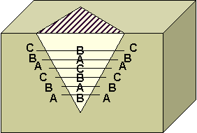
  • Stalking faults - extra or missing plane of atoms (for example ABCABC is the correct order, a stalking fault would be ACABC, in which the plane B is missing - see picture below)

    • Cause: they propagate from dislocations or oxides (impurities) from the surface
    • Grow in the film as an inverted pyramid (see picture)
    • Can be seen on the surface

  • Dislocations - are the 2D analog - line defects
    • Caused by lattice misfit, stress at the thickness where incommensurate growth starts
    • Cannot be seen at the surface, can be observed by selective etching which is a distructive method
    • They move by gliding/sliding
    • There are two types, depending on how they move: edge (the whole plane moves in the same time) and screw (the movement starts from a corner)

1. Theory of crystal growth
2. Various epitaxy methods

pages: previous | 1 2 3 4 5 [6] 7 8 | next

go to top