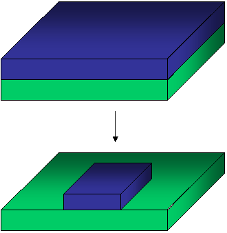
The task is to make MOS capacitors with square shape. The silicon wafer is oxidized and aluminium was deposited on top by PVD. You need to pattern the aluminium into squares of 1 μm x 1 μm. Make a plan of 10 steps for this task. Put them in order and indicate the processing details you need to write down: baking time, exposure time, developing time, etc. Consider also the following:
-
Choose the lithography and material type suitable for mask fabrication
-
Considering the fact that the mask will be used for a large number of times and the resolution is quite high, which type of lithography is suitable for patterning the aluminium squares, and how large should the gap mask-wafer be? Explain. Indicate also what are the resolution and DOF with this type of lithography? Lithography transfers a pattern from a mask to a substrate, via interaction of photons or particles with materials.
 |

 Substrate preparation