heating the substrate, although this method must be used with care, due to the fact that:
reactions may occur at Al/Si interface due to high temperature and a barrier material may be required between the two materials (Al and Si) to avoid reactions
the grain structure is modified by the temperature, grains can be bigger and the resulted film can be rougher
force fill
biasing the substrate - bias sputtering
A bias is applied on wafer in order to atract Ar ions and:
clean the substrate and remove native oxide
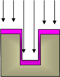
sputter deposited material in the trench and redeposit it on the sidewall, like in the picture below
Disadvantages of bias sputtering:
the films may have higher roughness due to the succesive processes of deposition and sputtering
the film can get damaged for high biases, due to bombardment with high energy Ar ions
introducing a collimator - collimator sputtering
the collimator has the purpose to select only the atoms that arrive perpendicular on the substrate, stopping the atoms which arrive at higher angles
Disadvantages of collimator sputtering:
deposition takes place also on collimator, thus the collimator has to be replaced periodically
low deposition rate on substrate due to the selection process
reduced sidewall coverage (see picture below)
Ionised metal plasma
Sputtered atoms pass trough a plasma and become ions
Ions arrive at substrate, are neutralised and deposited

 Substrate preparation