IPCI logo
Internet-based Performance Centred Instruction
Accelerometers tutorial

Modules

1. Introduction to Acceleration Measurement
2. Piezoresistive Accelerometers
3. Capacitive Accelerometer

pages: previous | 1 2 3 [4] 5 | next

Three-axis piezoresistive accelerometer:

Basic features:

  • Commercial 0.8 μm CMOS technology was used
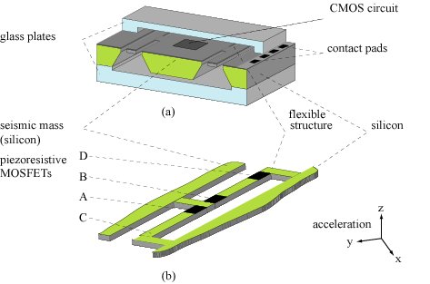
  • Three-layer structure formed by cap glass, micromachined silicon and bottom glass
  • Detection of three-axis acceleration, and signal processing to extract each component of acceleration,
    are performed by the on-chip CMOS circuitry
  • Signal processing circuits are formed by a commercial 0.8 μm CMOS technology
  • For detection of acceleration, p-MOSFETs are used as stress sensitive elements
  • Sensing principle is based on piezoresistive effect of p-type inversion layer in p-MOSFETs
  • Since p-MOSFETs are standard elements in CMOS circuits, it is convenient to use them
    in CMOS integrated sensors as sensing elements
  • Piezoresistive coefficient of p-MOSFETs does not strongly depend on the CMOS technology used
  • Piezoresistive coefficient of conventional piezoresistors is quite sensitive to their impurity concentration
  • One of four sets of folded beams surrounding the seismic mass is shown in the part b of the preceeding figure
  • Folded beam was designed to have the maximum sensitivity in a die size
  • Four sensing p-MOSFETs are formed on the folded edges of each beam where the largest strain
    is generated by beam deflection
  • Sensing elements are put at a distance from the boundary in order to minimize the strong variation of the sensitivity
    that occurs near the folded edge of beams
  • Device performance of this accelerometer is not so sensitive to device fabrication error
  • Sensing p-MOSFETs in this accelerometer are standard p-MOS devices formed in the commercial
    CMOS fabrication process
  • Gate size of p-MOS piezoresistor devices is 45 μm in length and 140 μm in width, respectively
  • Area of gate was designed to be relatively large so as reduce 1/f noise from them.
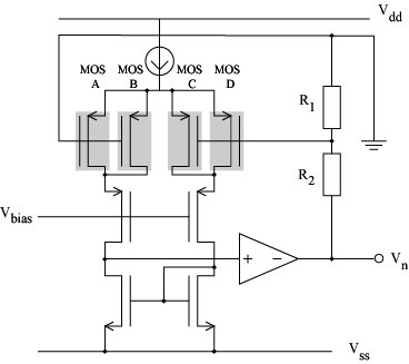
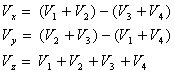
  • Stress detection circuit using the four sensing p-MOSFETs on each beam is shown in following figure:

  • Each detection circuit can detect the direction (polarity) and amplitude of deflection at the centre of each beam structure

  • Detected strain signal is amplified by the detection circuit at the same time

  • If the centre of the beam (connection point with the mass) is moved upwards from the chip surface,
    generated stress becomes:

    • Tensile on MOS-A and MOS-B

    • Compressive on MOS-C and MOS-D

  • Differential mobility change occurs between the two MOSFET pairs in the input stage of the differential amplifier
    due the piezoresistive effect in p-MOS inversion layer

  • Output voltage of the detection circuit for each beam Vn (n = 1..4) is expressed by the following expression:

  • In this expression:

    • A total voltage gain of the amplifier

    • Voffset input offset voltage of the amplifier induced by stress

    • C constant which depends on circuit design

    • ppMOS piezoresistive coefficient of the p-MOSFET

    • sAB induced stress on MOS-A and MOS-B

    • sCD induced stress on MOS-C and MOS-D

    • Tin translation constants between induced differential stress on each beam, n
      and each component of input acceleration in the direction i

    • ai component of input acceleration vector in the direction i

  • Three-axis components of acceleration are calculated from the signals of the four detection circuits
    by using the following expressions:

  • Accelerometers reported in literature:
    • Accelerometer with dimensions 3 x 3 mm2 having the sensitivity of 2.45 mV/g in x and y axis and the sensitivity of 12.5 mV/g in z axis
    • Accelerometer with dimensions 6 x 6 mm2 having the corresponding sensitivities are 31 mV/g and 167.5 mV/g, respectively.

1. Introduction to Acceleration Measurement
2. Piezoresistive Accelerometers
3. Capacitive Accelerometer

pages: previous | 1 2 3 [4] 5 | next

go to top