has low thorughput, is used for direct writing (not though a mask), thus the wafer is not exposed at the same moment, but each region is exposed separately, thus it takes a longer time
Masks for photolithography are written in the same way (direct writing with EBL)
Write and projection systems
A simple type of mask can still be used to increase the throughput, in some cases:
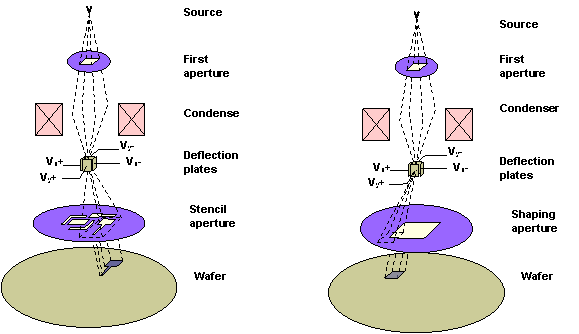
Stencil mask is used when on the wafer must be written similar structures (see left picture)
Square aperture - used for making segments of different size and orientation (see right picture)
Raster and Vector
The wafer is scanned, the beam covers the whole wafer - raster scan
In order to improve the throughput, the beam can write only in some areas/directions, in which is required, instead of scanning the whole wafer - vector scan

 Substrate preparation