a high electric field is applied between the tip of the probe and the surface
HO- ions diffuse due to the electric field into the material and oxide is grown where the is placed
the oxide grown is localised to a very small spot - high resolutions can be obtained
the distance between the tip and surface is controlled as in AFM by system comprising of :
cantilever - the arm of the probe
optical lever deflection sensor, which senses the position of the tip by measuring the reflection of a laser beam on top of the probe
scanner to modify the tip position mechanically
the current measured between the probe and the surface (for conductive surfaces) gives information on how much force should be applied in order to maintain the distance constant
carbon nanotubes can be used as tips for SPL
they are conjugated carbon molecules having delocalised p-electrons
can have diameter in the order of nanometers - very small
they can add material or etch it from a surface - nanotubes are very hard from the mechanical point of view
Dip-pen lithography
is similar to SPL, done also with an AFM tip
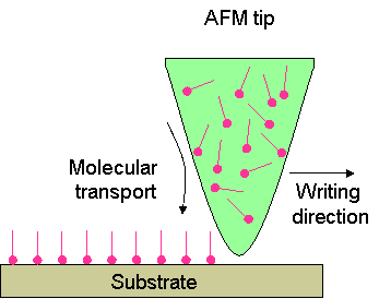
the tip has the property that material can be inserted in it (like ink in a pen) and when it is brought close to a surface, the material from the tip is "written" on the surface

 Substrate preparation