 |
|
||
|
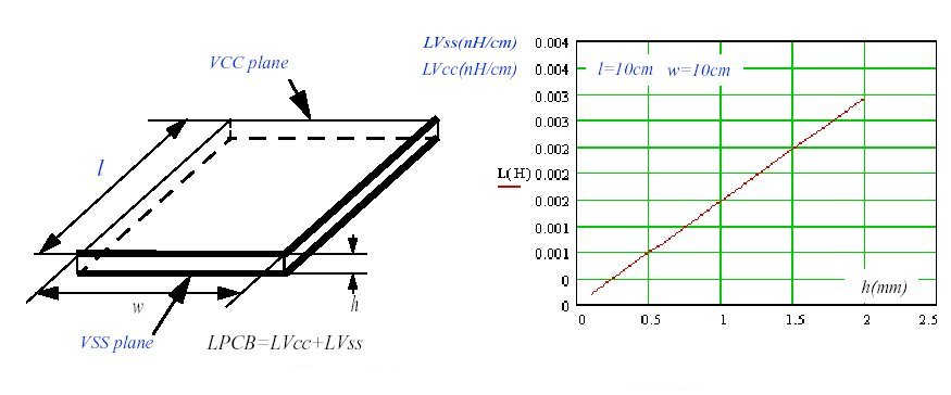
These planes are not very efficient in low frequency because the equivalent capacitor is not so high and the impedance across the circuit increases and the emission levels, too (figure 7/17). In low and medium frequency ranges additional decoupling capacitors help to maintain this impedance low.
Fig. 7 PWR(VCC)-GND(VSS) planes characteristics Table 1 shows the value of the PCB inductance for the three configurations seen above. The PWR and GND plane configuration gives the best result and a quite large decoupling capacitor.
Tab. 1 Comparison of PCB inductances (wt= 1mm, w= 10cm, l= 10cm, h=1.6mm)
|
 Schematic design of PCB projects
