 |
|
||
|
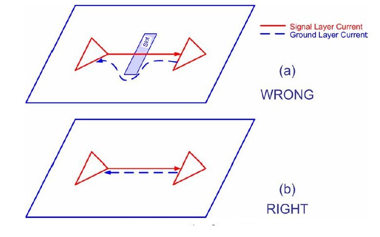
It can be said that a ground plane is a fundamental printed circuit structure used to combat transient (parasitic) phenomena, which are EMC phenomena. The use of "buss wire" is (totally) unacceptable as a "ground" because of its impedance at the equivalent frequency of most logic transitions. For instance, #22 gauge wires have about 20nH/inch inductance. A transient current having a slew rate of 10mA/ns created by a logic signal would develop an unwanted voltage drop of 200mV at this frequency flowing through 1 inch of this wire. For a signal having a 2V peak-to-peak range, this translates into an error of about 200mV, or 10% (approximate 3.5-bit accuracy). Even in all-digital circuits, this error would result in considerable degradation of logic noise margins. Using a solid plane for ground solves many problems simultaneously. A solid plane provides a low-impedance between all the ground points whilst allowing return currents to travel directly underneath their respective signal traces. A common mistake made by PCB designers is to use holes, voids and slots in the ground plane (figure 4). Figure 4a shows the current flow when a signal trace is routed over a ground plane slot. The return current is forced around the slot, thus creating a larger loop area. Figure 4b shows the current flow without a slot in the ground plane. Notice how the loop area is kept to a minimum.
Fig. 4 A common mistake in PCB designs: holes, voids and slots in the ground plane
|
 Schematic design of PCB projects

