 |
|
||
|
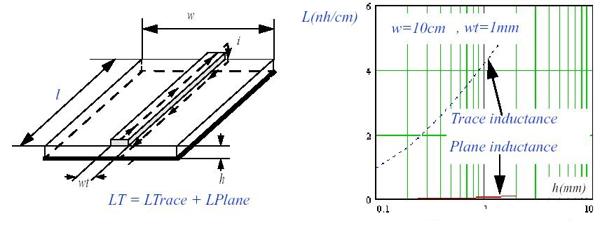
The total inductance of a loop (LT) is drastically reduced when using a GND plane because the equivalent inductance of the plane (Lplane) is much lower than the PCB trace (Ltrace) as it shown in figure 5. Fig. 5 The total inductance of a signal loop (LT) is drastically reduced when using a GND plane This is mainly due to the contour taken by the H field which is much larger than the contour taken around the signal trace. These two inductances are rather independent and be evaluated separately. The ground plane inductance is not affected by the PCB trace width and can be evaluated using the following expression:
The PCB trace inductance can be evaluated using the following expression:
This inductance is independent of the PCB ground width. For example a trace of 10cm length and 1mm width and separated from the ground plane by 1.6mm presents an inductance of 51nH. A plane with the same dimensions and 10cm width presents an inductance of 0.8nH. So, the total inductance is the sum of the PCB trace and plane (51.8nH).The same trace without the ground plane has an inductance equal to 115nH. So thanks to the plane the trace inductance is reduced down to 2.5 factors.
|
 Schematic design of PCB projects


