 |
|
|
Aims
"PCB Design" is a task based multimedia course which provides the students with a systematic presentation of high performance printed circuit/wiring board (PCB/PWB) design and complex characterization of PCB structures and offers, based on numerous figures, formulas and examples, a practical approach on design of printed circuits. The objectives of this course are the following:
1) Understanding main topics of printed circuit/wiring board (PCB/PWB) design.
2) Understanding the CAD design flow for PCB electronic modules development.
3) Understanding the principles of analog and digital PCB designs.
4) Understanding advanced topics in PCB design based on electromagnetic compatibility, signal integrity, and related issues.
5) Understanding PCB post-processing and the interface designer - manufacturer.
Contents
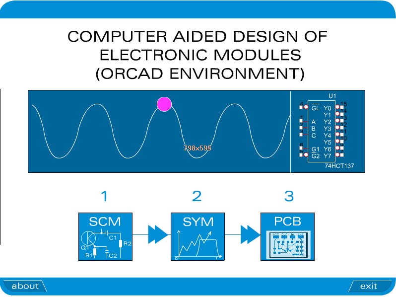
The course is destined to cover both theoretical aspects related to PCB design and practical aspects for computer aided design of PCB. It is based on two main tasks. The first one is destined to the design of an analog PCB electronic module and the second one to the design of a digital PCB module. In order to understand the fundamental topics of PCB design, the student can download a general tutorial from the address:
http://www.ipci-project.com/files/tutorials/images/16/MMPCB_tutorial-total.zip
This tutorial is divided in two main areas: "Fundamentals of PCB design" and "CAD for PCB". The eight modules, four destined to "fundamentals" and four to "CAD" cover a large area of topics, from basics of PCB design to signal integrity analysis, simulation, design techniques and CAE-CAD tools. Additionally, the student shall find a multimedia glossary of terms, animated design flows and practical tasks, various types of tests for creating a solid background for future engineering activity in PCB field. "Fundamentals of PCB design" covers theoretical fundamentals of printed circuit structures design. It starts with basics of PCB, structures and materials. The next chapters are oriented to an introduction in time, frequency and distance, PCB parasitics, lumped/distributed circuits, current capacity of traces, transmission lines, characteristic impedance control, and termination technique. In addition, signal integrity analysis topics, as relative permittivity/effective permittivity, reflections, and crosstalk and EMI are discussed in depth. "CAD for PCB" covers the basics of CAD-Computer Aided Design in development of PCB. The course presents techniques and methods for placement, routing, and optimizing the PCB. The last part is destined to CAD-CAM systems for post-processing, Gerber/Excellon files generation, and interfacing designer and fabricator. The CAD area is based on OrCAD and supports all the phases of the design process: design creation, placement of footprints, routing of traces, post-processing, and inter-tool communication. |
|
The course is based on OrCAD/Windows design environment due to its high quality features in CAD conception of electronic projects and powerful printed Circuit Board (PCB) design of on-board metallic interconnection structures. The environment supports all the phases of CAE-CAD-CAM design process using the internal native blocks of OrCAD or external blocks which are basically stand-alone programs and are provided by other professional companies as Wise (Gerbtool), Quantic (Omega Plus) and Cadopia (IntelliCAD).
(source:www.vutrax.co.uk)
The PCB design flow allows the following main activities: SCM design creation, SCM post-processing, placement of components, routing of tracks, optimizing the final layout, PCB post-processing, and Inter-tool communication (for various links between blocks).
Below is offered a "zip" archive of a Flash presentation that emphasize the basic design flow of a PCB electronic module.
http://www.ipci-project.com/files/tutorials/images/16/CAE-CAD-CAM_Practice.zip
Using the schematic block "OrCAD Capture" the designer can create the Layout-compatible netlist that includes preset design rules to guide logical placement and routing, depending on the type of the electronic project (analog, digital, mixed, high density, high speed). SCM gives the ability to specify critical design rules at the schematic level (component locations, spacings, grouping of components, widths of signal and reference tracks, routing layers, etc.) and bring them into Layout inside the netlist SCM-PCB transfer file. Layout's Auto ECO (engineering change order) procedure from Layout updates the PCB design without destroying a finished layout work.
In OrCAD the user can perform manual placement or interactive/automatic placement utilities of components, having a total control of the component placement process. During auto-placement, Layout can use the powerful 'shove' capability to move components out of your way automatically while keeping the guidelines of various design rules (DRC).
The same for routing, the user can perform manual routing or interactive/automatic routing of conductive PCB tracks. Using manual route it is possible to guide the routing process based on specific requirements (track by track). In interactive routing, the designer still control the routing of individual tracks, but can take advantage of Layout's automatic routing motors, such as 'push & shove' capability (it allows to move pre-routed tracks in order to create space for the current track). The auto-router can route singular tracks, selected areas inside the layout, groups interconnections (nets), or the entire printed circuit board.
At the end of PCB stage all of output settings are stored in a spreadsheet that the user can recall and revise. It is possible to give layer-by-layer instructions for writing Gerber (standard and extended), Excellon, DXF and other formats of files, as well as hardcopies in order to generate the technical documentation. A large range of of reports (BOM, DRC, drill lists, parts orders, ECOs, fabrication & assembly drawings, pick-and-place info, etc.) can be easily produced.
OrCAD has the capability to communicate interactively inside its environment (Capture & Layout) using the feature called 'INTERTOOL communication' to communicate updated SCM information to Layout, at any stage of the design process and to 'BACK-ANNOTATE' PCB design data to Capture. Intertool communication supports cross-probing to facilitate design analysis (selecting a signal or part in Capture/Layout, the corresponding signal or part is automatically highlighted in the other block). |
|
- Passive Electronic Components and Structures
- Active Electronic Components and Devices
- Analog and Digital Integrated Circuits
- Basics of Electronic Packaging
- Basics of PCB |
|
 Task 1: Schematic design of PCB projects Task 1: Schematic design of PCB projects
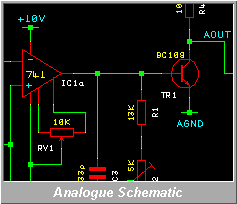
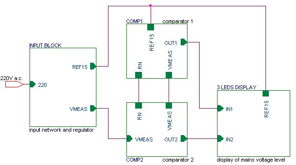
The task consists in the SCM design of the two PCB projects necessary to be developed in this course (the analog and digital modules, described in tasks 2 and 3) and understanding of the schematic capture flow which has to be followed in order to create the circuit diagrams for both projects. Task 2: Design of a PCB analog module Design a PCB analog module which supervise the AC power supply voltage of mains and indicate based on 3 LEDs (one red LED for over-voltage, one red LED for under-voltage and one green LED for OK-working) if the voltage is into the correct range (210...250V). The current of LEDs shall be of 10mA. Use comparators/operational amplifiers in an optimim number and packaging and try to find a solution for the DC power supply of integrated circuits in order to use no transformer.
Remark: For 'beginner' level in PCB design, the tutor can offer to student the schematic diagram of the task.
Requirements for the printed circuit board:
- Single-layer PCB (bottom side);
- More than 50% of components as SMDs, inclusive the comparators (SOIC is preferred);
- PCB tracks: min. 0.5mm, rounded corners;
- Spacings: min. 0.5mm;
- AC power supply voltage bars: min. 2mm;
- DC power supply of integrated circuits: 15V, PCB tracks of 0.8mm;
- Board: rectangular in shape, with 4 mounting holes of 3.2mm at corners;
- Components density (Area of components/Area of board) > 40%.
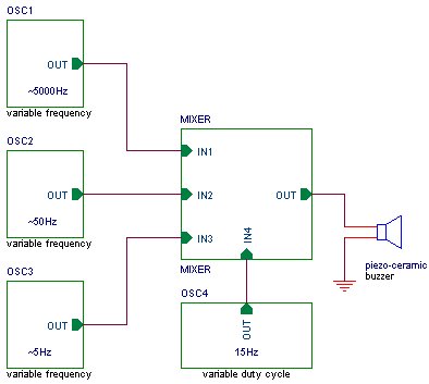
Task 3: Design of a PCB digital module Design a PCB digital module in CMOS technology which generate a continuous burst audio sound based on 4 oscillators (see the block diagram from below). The first three are trigger Schmitt oscillators, each one being designed with a single CMOS gate. The last oscillator is a classical one, with 2 CMOS inverters, and must have a variable duty cicle. Place at the output a piezoceramic buzzer in order to avoid the usage of an audio amplifier and a loudspeaker. Find the optimum solution in order to use only two integrated circuits.
Remark: For 'beginner' level in PCB design, the tutor can offer to student the schematic diagram of the task.
Requirements for the printed circuit board:
- Double-layer PCB;
- All components as SMDs;
- Signal PCB tracks: 0.3mm, mitered corners;
- Spacings: min. 0.3mm;
- DC power supply of the module: 6V, PWR tracks of 1mm;
- GND structure: partial metallic plane placed onto bottom side, having a gap of 1mm to the interconnection structure;
- Board: circular in shape (4cm in diameter), with 1mounting hole of 6mm in the middle of the board;
- Components density (Area of components/Area of board) > 55%;
- A text (entitled TASK 2) placed onto the top electrical layer, written with copper, and having the parameters: height= 2.54mm, trace width= 0.5mm.
Task 4: Solving EMC and SI Issues Based on this task the students shall be able to understand some specific topics of advanced PCB design and to have a global engineering view and professional skills regarding real projects.
Strongly based on practical engineering aspects, the task offers a basic background for a future design and research activity in electronics engineering and CAE-CAD-CAM area for development of printed circuit boards. Task 5: PCB post-processing Post-processing activities are fundamental operations, at the end of a printed circuit board design, which create the link between the designer and the manufacturer. The files generated (usually in Gerber and Excellon formats, plus reports associated to them) allow the driving of manufacturing equipment of real printed circuits. |
|
|
|

 Schematic design of PCB projects