 |
|
||
|
After post processing, the artwork plot will look like the figures below:
Examples of drill drawings inpost-processed in CadStar (left) and Orcad (right)
IV. POWER PLANE (PP)
The name is destined for any reference plane, power and ground, placed into a ML-PCB. Having reference planes into a printed circuit board represents the best solution for minimizing electromagnetic interferences and for creating a PCB electronic module with higher immunity and a lower electromagnetic pollution. Power plane is of two types:
· Copper components; · Routes; · Via; · Drawn pads; · Teardrops; · Copper;
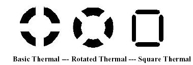
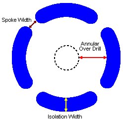
For power and ground plane post-processing, there are two types of pads: 1. Connected to the plane (based on a special PCB item named "thermal relief);
Thermal relief item in Orcad environment
In the figures from above the reference plane and the thermal relief pads are presented "in reverse". The white areas represent copper and the black/blu isolations into the plane. It can be observed 4 conductive bridges (called sometimes "wheel spokes") which create the electrical connection of a thermal relief pad to the reference plane. Thermal relief pads are used as contacts to plane layers or copper zones, for applications such as the connection to power and ground on a multilayer board. There are two things a designer must do before defining thermal reliefs: · designate the target layer for the thermal reliefs as a plane layer in the Layers spreadsheet · assign a net to the layer. Of course, we could make a good solid connection by just completely eliminating that Thermal relief pad. But this condition causes problems in soldering anything into that hole, like a component lead, because it gives a high thermal conductivity that tends to suck away the heat from the hole too rapidly, causing poor solder melting and possible a cold solder joint. The wheel spokes give a reasonable compromise between limited thermal conductivity and good electrical conductivity between the bulk of the copper plane and the plating barrel.
2. Not connected to the plane. The hole in plane around a pad non-connected to the plane represents an antipad. So, it is an insulating hole/annulus (ring) in a plane layer when there is no connection between the plane and the hole. On the screen or a Gerber plot in negative image, it usually appears as a black or colored pad/annulus with an inside diameter larger than the drill diameter. On a normal routing layer (not a plane layer), any hole will have a copper pad which is larger than the drill size. If there is no connection within this layer, this ring gives added strength and anchorage to support the copper cylinder that's plated onto the surface of the hole. If there is a trace connection, it gives a robust all-around electrical bonding. Often, for top and bottom routing layers the pad will be made larger for added strength and to resist possible peeling away from the board surface. The ring is no-copper and all the rest is copper - copper inside the ring for the supporting pad that gets connected to the plating barrel, and copper outside the ring that's the undisturbed metal of the plane. A via represents a special case because we normally don't expect to solder anything to it. For a via that's not connected, we would see a normal ring antipad, assuming we still want that anchoring support for the plating barrel. So, for this case we would see a colored ring around the via.
|
 Schematic design of PCB projects