IPCI logo
Internet-based Performance Centred Instruction
Basics of PCB post-processing tutorial

Modules

1. Introduction
2. Equipment types
3. Post-processing versions
4. Practical post-processing activities

pages: previous | 1 [2] 3 4 | next

Post Processing for SM


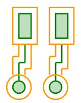
All pads and vias are oversized with a value into the range 5...20 mil in order to create a correct SM film, with a small gap between it and the pads via.


Top (bottom) electrical layer having the interconnection structure onto it


SM Generation

  1. Post-processing of the electrical layer from above based on an "oversize" procedure for all the pads (and vias, usually) and obtaining the first plot.

Oversized pads (with yellow); even also for tracks is  an "oversize" presented (as a theoretical enlarging of all the items), they shall remain with the same width


  1. Photo reversing the plot from point 1 without taking into account the traces. A SM plot will be generated, having windows around all pads and via (like in the figure from below, yellow outline).


Solder mask of the top (bottom) electrical layer having the interconnection structure onto it

1. Introduction
2. Equipment types
3. Post-processing versions
4. Practical post-processing activities

pages: previous | 1 [2] 3 4 | next

go to top