 |
|
||
|
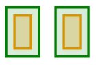
Solder Paste Mask (SP) Solder paste mask is a non-electrical mask destined only for layouts with SMD (Surface Mounted Device) and is used for placing solder paste onto all SMD pads (land patterns). SP is generated only for SMD components using an "undersize" procedure in order to obtain small windows, with the same shape as the land patterns but with smaller dimensions (see the figure from below).
Based on the SP a stencil is manufactured for placing the solder alloy onto the board, at right locations of SMD pads.
Solder paste mask (yellow outline is the contour of the holes into the mask)
Silk Screen (Silk Mask) Silk Screen (SS) is a non-electric mask destined for inscription the PCB and for specifying information regarding the electronic components which have to be placed onto the board. It usually contains information about company, texts and figures.
I. DRILL DRAWING Drill drawing is an artwork plot destined for technical documentation which specifies the right location off all the holes in the frame of PCB and the size of the drills. After post processing a drill report is released. For blind and buried via this report contains different drilling files for different pairs of layers (in the case on ML-PCB).
Drill drawings can have informative text for the manufacturer where is specified the drilling sequence. This file is ASCII type file and is read if it is introduced in ANNOTATION FILE area from DRAWING OUTPUT menu.
Drill associated report released after post processing
|
 Schematic design of PCB projects