 |
|
Crystal orientation
Usually the susbtrates are crystalline materials. The crystal orientation depends on how the wafer was cut in relation with the crystal lattice.
-
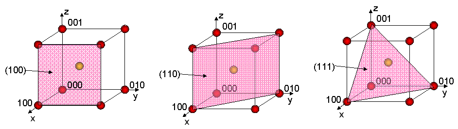
Miller indices, written as (110) for example, are used for indicating the crystal orientation. Miller indices of a plane (x,y,z) show where the cutting plane (surface) has intersected the three axes: Ox, Oy and Oz (see the picture above).
-
The differences between wafers with various crystal orientations are caused by the packing densities. In a crystal cell, like the one presented in the picture above, atoms may be situated in the nodes, planes, lines. Depending on how you are looking (i.e. how the wafer was cut), the atoms may be closer packed or not. For a (111) Si crystal, for example the carrier mobility is lower than for a (100) Si crystal. Other processes such as chemical reactivity, crystal growth, diffusion depend also on the crystal orientation.
-
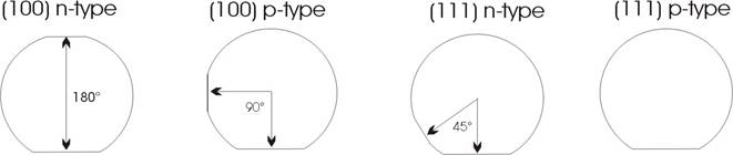
The wafer type and orientation can be recognised by the flat positions (which were cut during the substrate fabrication). There are two types of flats:
-
Primary flat (the longest flat, is perpendicular on 110 direction)
-
Secondary flat (its position depends on crystal orientation)
-
Below are shown how you can recognize different type of wafers based on the flat positions
|
|

 Substrate preparation
