Each type of wafer has different electrical, mechanical and optical properties.
The material is selected in order to be suitable for the application. Thus, in order to
choose the appropriate wafer, the application has to be known.
A few types of materials used for substrate fabrication are shown below:
-
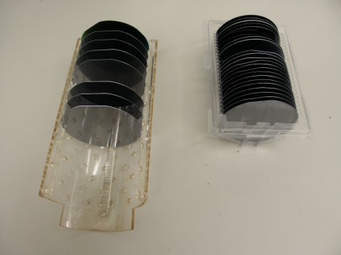
Silicon
-
Germanium
- Used in the beginning for transistor fabrication
- Properties:
- higher mobility than silicon
- not good natural oxide - maybe in the future, if high-k dielectrics are introduced as gate dielectrics
- compatibility with III-V compounds (Ge has a direct bandgap)
- Applications: epitaxial growth of III-V compounds.
- SiC in micromachining (MEMS), brittle, cannot suffer plastic deformations due to covalent bonds
- Properties
- extreme hardness
- high temperature resistance
- radiation resistant
- less elastic than Si, brittle
- Applications:
- micromachining (MEMS)
- high-power/high-frequency devices
- electronic devices
- GaAs
- Second most common semiconductor material
- Properties
- direct bandgap semiconductor (electrons and holes can recombine directly without requiring a phonon, the probability is much higher thus for direct transitions across the bandgap than for the indirect ones)
- higher electron mobility than Si
- lack of natural oxide
- Applications
- monolithic microwave integrated circuits (MMICs)
- semiconductor laser applications
- LEDs
- FETs
- OMEMS
- Glass
- Applications:
- for displays
- wafer bonding
- low temperature applications
- Plastic
- Properties
- flexibility
- ultra-lightweight
- durability
- cost-effective processing
- Applications:
- Biodegradable organic for medicine applications

 Substrate preparation