IPCI logo
Internet-based Performance Centred Instruction
Substrate selection and fabrication tutorial

Modules

1. Wafer material
2. Wafer properties
3. Wafer fabrication
4. Wafer cleaning

pages: [1] 2 3 | next

Conductivity type

  • Atoms are introduced in the silicon network, in order to modify its conductivity/resistivity.
  • Silicon has four valence electrons. All the four electrons participate in covalent bonds with the four adjacent atoms in the silicon crystal lattice, as in the lower picture.
  • Some atoms have five electrons on the last layer (phosphorous). When a phospohorous atom is inserted into the Si lattice , four covalent  bonds will be created with the neighbouring Si atoms and an extra electron will remain. This electron can be removed easily from the atom and participate in the conduction process, increasing the film conductivity.
  • In a similar way, atoms with three electrons on the last layer will participate with a hole to the conduction process.


  • N-type:   Phosphorous, arsenic, antimony used as dopants         Electrons are the charge carriers 
  • P-type:    Boron used as dopant                                                                 Holes are the charge carriers

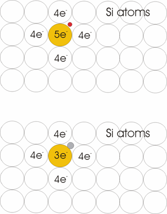
Resistivity

Gives information on how strong is the opposition of the material to current flow. The substrate resistivity is modified by doping (introducing atoms with 5 or 3 electrons on the last layer). It is an important parameter, because other processes speed (e.g. oxidation) are influenced by the substrate resistivity. Normal value: 1-10 ohm per cm2.

1. Wafer material
2. Wafer properties
3. Wafer fabrication
4. Wafer cleaning

pages: [1] 2 3 | next

go to top