the optics are arranged so that the image is formed clear in the center of resist thickness
if the resist is very thick, the image will be out of focus at the surface of the resist or at the interface with the substrate
the situtation appears where due to topology, the resist is thicker than usual
DOF is defined as the dimension (resist thickness) for which the image formed is still clear:
For systems with low DOF, planarization of the substrate is required
With increasing the resolution by increasing the NA of the system, DOF is severely decreased, thus a compromise between resolution and depth of focus is needed
a possibility is to use immersion lithography (the space between the mask and wafer is filled with water), which increases DOF for a constant low NA
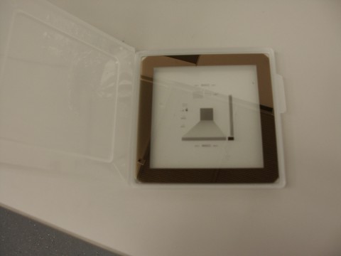
MASK - an example of a mask is given in the picture. Masks are fabricated with direct writting.
Stepper
The image from the mask is decreased and exposed on a part of the wafer. Then the position of the wafer is modified and the image is exposed again to the nearby region
Very high NA - high resolution
Disadvantage: throughput (more exposures are required for the same wafer)
Step and Scan
The wafer and reticle are moving, both are scanned in the same time, during exposure
Mask protection
Pellicle - to keep free of defects (particles are kept at a distance from the mask, thus they will be kept out of focus)
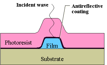
Antireflective coatings to avoid reflection of light
Reflections of light on mask or wafer can cause unwanted exposure (light is reflected in the regions which are supposed to be protected by mask) → hole in metal lines
Automatic inspection of mask defects
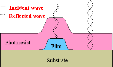
Standing waves
Created from interference of incident and reflected waves
Standing waves cause non-uniform exposure along the thickness of the photoresist film.

 Substrate preparation