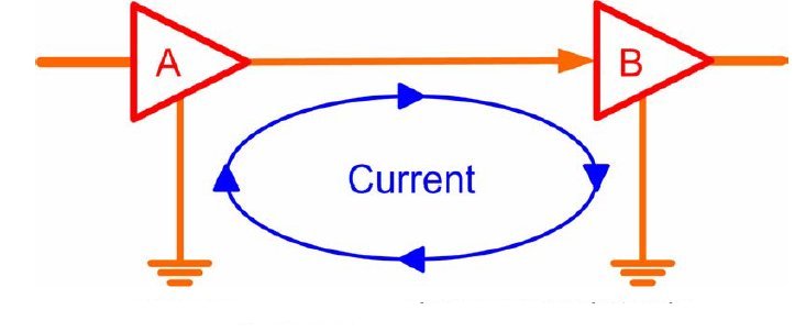
Fig. 3 A single-ended signal track for transmitting a signal between two gates
So, absolute all signals must have a return path back to the source. As frequency harmonics get higher, the path for the return signal will want to be directly underneath the signal trace. This can be on either a power or a ground plane. Taking a look to the figure 3, it is observed that the current flows into a loop (this is the, so called, “concept of the signal loop”. The signal trace and the return signal on the plane comprise a loop. If there is no obstruction anywhere on the plane, then the area of this loop will be small. If the return signal must take a circuitous path (the GND structure is not a plane, the GND plane is not solid, there are slots/voids into the plane, etc.), the loop area will be larger. EMI emissions are directly related to this loop area. Therefore, one reason for designing in planes is for control of EMI emissions. And one reason for avoiding slots and voids in planes is to minimize loop area.
