 |
|
||
|
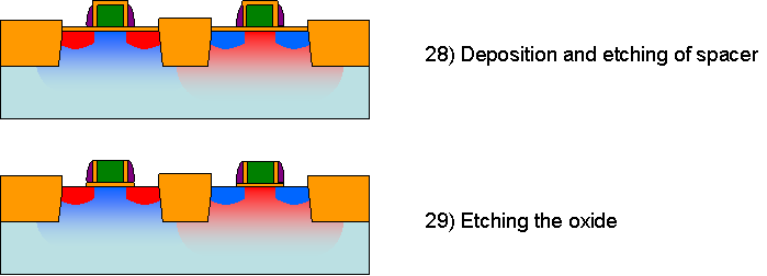
A nitride spacer can be deposited and etched (partially, due to less etching on vertical surfaces), forming the spacers. The spacers can serve also as masks for further implantation, but this is not shown in this simplified process flow. A metal (Ti) is deposited by evaporation and silicidation occurs on the Si surfaces (for a lower aheet resistance and to serve as barrier material between silicon and metal). The wafer is annealed and reactions occur between Si and Ti, creating TiSi2 (low resistivity). The metal deposited on dielectric, that has not formed silicide, is removed. Self-aligned silicide is fabricated this way. Dielectric is deposited for isolation.
|
 Substrate preparation


