 |
|
||
|
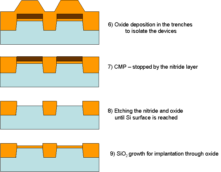
The isolation of the devices is completed by depositing silicon oxide in the trenches made before. The active areas of the devices are defined by etching the nitride mask. Also, a thin oxide layer is grown for the future implantation processes. The damage is decreased (due to collisions ion-surface) and the sheet resistance is also decreased (implantation peak is situated close to the interface oxide-silicon), if an oxide layer is used.
|
 Substrate preparation

