 |
|
||
|
Motion of free carriers in a semiconductor
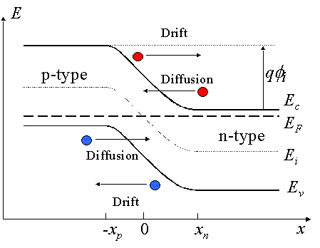
Thermal equilibrium Reached by the diffusion of electrons/holes close to the metallurgical junction across the junction into the p-type/n-type regions Depletion region is created - region depleted of mobile carriers Extends from x = -xp to x = xn Ionized donors and acceptors behind the depletion layer cause the electric field Causes the drift of carriers in the opposite direction Diffusion current balanced by the drift current - thermal equilibrium is reached Thermal equilibrium indicated by a constant Fermi energy
Built-in potential Internal potential, fi, equals the potential across the depletion region in thermal equilibrium Equals the difference in the Fermi energies, EFn and EFp, divided by the electronic charge Equals also the sum of the bulk potentials of each region,
Thermal voltage
Electron charge q = 1.6 10-19 C
Boltzman's constant k = 1.38 10-23 JK-1
Intrinsic carrier density:
function of the effective density of states in the conduction and valence band, and the bandgap energy Eg = Ec - Ev:
Bias voltage
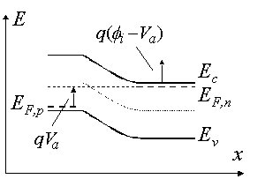
Application of a positive voltage to the anode (p-type region) Potential across the semiconductor decreases Depletion layer width decreases
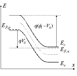
Application of a negative voltage to the cathode (n-type region) Potential across the semiconductor increases Depletion layer width increases
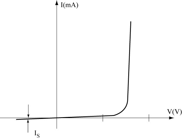
Current versus voltage characteristics of a p-n junction diode
Mathematical approximation:
IS ... saturation current Vt ... thermal voltage
|
 Analogue filter


 (Vt = 25.86 mV for T = 300K)


