Semiconductors
Silicon, germanium
-
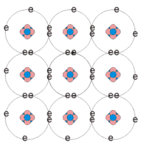
At very low temperature:
-
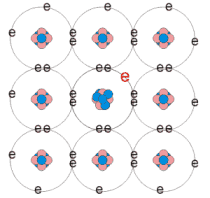
At room temperature:
-
Some electrons escape from the bonds due to the thermal vibrations
-
Conductivity lover than in metals
-
Resistivity: 10 -4 < r < 10 8 Ohms m
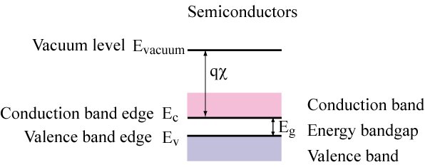
Energy gap typically around 1eV

Vacuum level (Evacuum) ... energy of a free electron outside the crystal
Quantified by the electron affinity (c) multiplied by the electronic charge (q)
Elemental semiconductors
-
Each atom is of the same type (Ge, Si)
-
Atoms bound together by covalent bonds
-
Each atom shares an electron with the nearest neighbour - strong bonds
Compound semiconductors
-
Made of two or more elements (GaAs, InP)
-
III-V semiconductors (elements from the group III and group V of the periodic table respectively)
Intrinsic semiconductors
-
Pure semiconductor material
-
No impurity atoms
-
Elemental and compound semiconductors can be intrinsic
-
Free electrons (n)
Electrons having enough energy to escape the electrostatic attraction from their parent atoms
-
Holes (p)
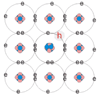
Vacancy left behind free electrons
May be filled by another electrons
Second carrier of positive charge
-
Same number of free electrons as holes (n=p)

Extrinsic semiconductor
-
Doping process
Adding impurity atoms to the intrinsic semiconductor crystal
-
Example: Silicon
Group IV of the periodic table - 4 valence electrons
Each atom shares an electron with a neighbouring atom
p-type extrinsic semiconductor
Acceptors - dopant atoms from the group III of the periodic table
(B, Al, In, Ga) incorporated into the crystal
Doping proportion 1 in 106
Insufficient number of bonds with the surrounding silicon atoms
Creation of holes - positive charge carriers

n-type extrinsic semiconductor
Donors - dopant atoms from the group V of the periodic table
(As, P, Sb) incorporated into the crystal
Doping proportion 1 in 106
Extra electron in the valence band - negative charge carriers

Resistivity of semiconductors
To include the contribution of electrons as well as holes to the conductivity,
we add the current density due to holes to that of the electrons, or:
J = qnve + qnvh = q(nn + pp)E
Conductivity s = J/E = q(nn + pp)
Resistivity r = 1/s

 Analogue filter

