p-n junction (p-n diode)
Structure

-
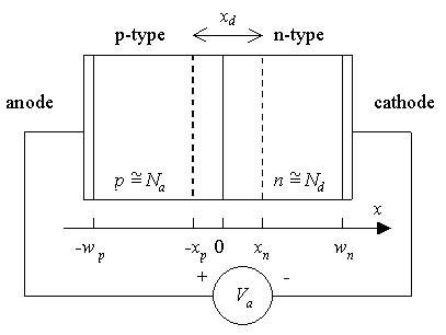
Two semiconductor regions with opposite doping type
-
Region on the left is p-type with an acceptor density Na
-
Region on the right is n-type with a donor density Nd
-
Electron (hole) density in the n-type (p-type) region is approximately equal to the donor (acceptor) density (shallow dopants)
-
Transition between the two regions is abrupt - abrupt p-n junction
-
Anode - contact to the p-type region
-
Cathode - contact to the n-type region
-
Junction is biased with a voltage Va
Principle of operation

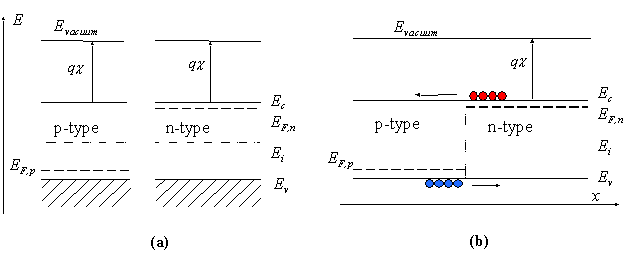
Figure a)
Energy band diagram of a p-n junction before merging both semiconductor regions
Figure b)
Flatband diagram - obtained when both semiconductor regions merged together
and conduction and valence band energies of each region aligned
Fermi energy - strictly associated with a particle, which is in thermal equilibrium with the system of interest
(does not consist even in part of heat or work)
often called the electro-chemical potential
EFn, EFp ... Fermi energies - not automatically aligned
Flatband diagram is not an equilibrium diagram
both electrons and holes can lower their energy by crossing the junction

 Analogue filter


