IPCI logo
Internet-based Performance Centred Instruction
MOS Transistor tutorial

Modules

1. Semiconductor Physics
2. MOS Structure
3. MOS Capacitor and Switch
4. Small-signal Operation of MOSFET
5. CMOS Technology Nodes

pages: previous | 1 [2] 3 4 5 6 7 | next

Electrical conductors

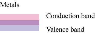
  • Metals (aluminium, copper, silver, ... ), graphite
  • Atoms arranged in a regular crystal array
  • Large number of atoms
  • High conductivity
  • No forbidden gap
  • Conduction and valence gap overlap


  • Conductivity of a material
    defined as the current density, J,  divided by the applied electric field, E
  • Current density
    product of the charge of the mobile carriers, q,  their density, n,  and velocity, ve
    can be expressed as a function of the electric field using the mobility, n:

  J = qnve = qnnE

  • Conductivity  s = J/E = qnn
  • Resistivity  r = 1/s = 1 / (qnn)


1. Semiconductor Physics
2. MOS Structure
3. MOS Capacitor and Switch
4. Small-signal Operation of MOSFET
5. CMOS Technology Nodes

pages: previous | 1 [2] 3 4 5 6 7 | next

go to top