IPCI logo
Internet-based Performance Centred Instruction
Advanced lithography tutorial

Modules

1. Electron beam lithography
2. X-ray lithography
3. Ion beam lithography
4. Nanolithography

pages: [1]

  • X-Ray Lithography
    • Wavelength very low - lower than a few nm
    • Resist, usually PMMA, is exposed through an x-ray mask in proximity or in contact with the wafer.
    • This technique has the advantage that very high aspect ratios can be achieved, since the x-rays are highly penetrating.
    • The wavelength of an x-ray is given by λ = 1.2/E(keV), so one would expect higher energies to be more desirable. However high energies can mean also damage on the film, special resist, etc.
    • Blur, caused by the excitation of photoelectrons and the associated shower of secondary electrons limits the patterning ability to about 20 nm.
    • XRL has been applied to MEMS, where the high aspect ratio is a distinct advantage.

  • X-ray sources
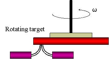
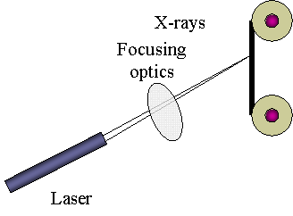
    • 2 sources of creating X-rays:
      • Electron bombardment
      • Laser
    • Synchotrons are also used for X-ray


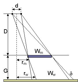
  •  Proximity X-ray exposure system
    • Difficult to make optics for X-ray
    • Problems:
      • Distortion:
        • Mask has to compensate
      • Shadow:
        • Reduces the resolution
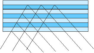
        • Optics can be used to produce a uniform wide-area beam (materials with low Z, high Z can be used as in the lower picture to reflect the beam)


  • Applications of X-ray litho: device patterns with feature sizes less than 40 nm achieved

1. Electron beam lithography
2. X-ray lithography
3. Ion beam lithography
4. Nanolithography

pages: [1]

go to top