IPCI logo
Internet-based Performance Centred Instruction
CAD techniques for PCB design tutorial

Modules

1. The PCB Layout design flow
2. Starting a PCB project
3. The Layout design environment
4. Setting up the virtual board
5. Creating and editing obstacles
6. Working with footprints and components
7. CAD procedures for placing and routing

pages: 1 2 3 | next

Layout supports every phase of the design process. A typical printed circuit board design flow has five key phases:

· Board-level schematic

· Component placement

· Board routing

· Post processing

· Intertool communication

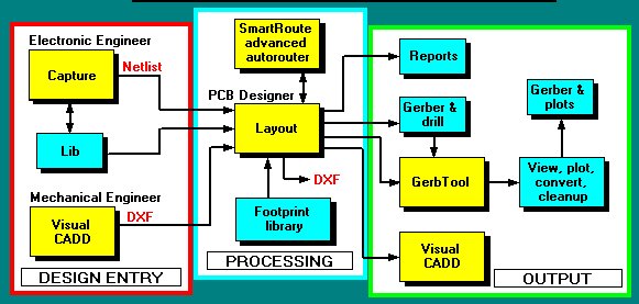
The block diagram of OrCAD PCB Layout environment is below presented.

Block diagram of OrCAD PCB Layout environment

1. The PCB Layout design flow
2. Starting a PCB project
3. The Layout design environment
4. Setting up the virtual board
5. Creating and editing obstacles
6. Working with footprints and components
7. CAD procedures for placing and routing

pages: 1 2 3 | next

go to top