 |
|
Bulk micromachining
-
is removal of a lot of material - almost the entire film thickness - to create windows, membranes, various structures
-
How - by etching:
-
Wet etching:
-
isotropic and undercut appears, which can be used in some devices
-
-
KOH - not compatible with ICs (alkali metal such as K contaminates the transistors); high selectivity for vdifferent crystal orientation: (100 : 111 = 400 : 1), silicon nitride is a very good mask (selectivity 1000), silicon oxide (selectivity 100), stops at p++ layers
-
EDP (ethylene diamnie purocatechol) - toxic, carcinogenic, lower anisotropy: (100 : 111 = 35 : 1)
-
N2H4 - explosive
-
TMAH (tetra methyl ammonium hydroxide) - the etch difference not so big: (100 : 111 = 25 : 1)
-
Dry etching:
-
Control of etch depth - in order to make structures with certain dimension, it is important to etch the right depth; there are a few methods used to control the etch depth:
-
Timing - it is the least accurate method, due to the fact that etching rate varies very much with temperature, concentration, etc
-
Anisotropic etching of v-grooves - if only small rectangulars/windows are made, then in an anisotropic wet etch, the etching stops when the two planes combine, making a V-groove
-
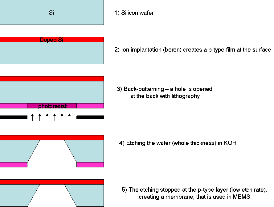
P++ doping - the etch rate is much lower in high doped material, than in undoped material, therefore if implantian occurs in the region where etching should end, an etch stop is created as shown below
-
explanation: electrons recombine with holes, limiting the electrons number needed for etching
-
Not IC-compatible, more process steps, lower piezoresistive coefficient for high doping
-
SiO2 (or other material) can be used to stop the etching
-
Electrochemical etch stop - by biasing positive a n-silicon part, the p silicon will be etched, the n-Si not
-
The picture below shows an example of bulk micromachining, how a membrane is created. SiO2 or Si3N4 can be used as masks for etching Si, but in the process flow it was not shown their deposition.
 |
|

 Substrate preparation