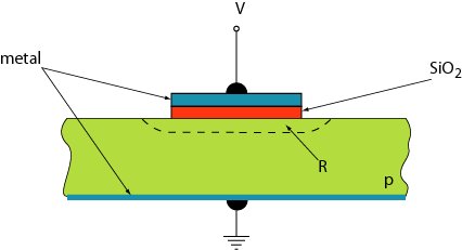
Metal-oxide-semiconductor (MOS) structure
Structure consisting of (from top to bottom)
-
Metal
-
SiO2 (insulator)
-
p-type silicon
-
Metal
Operation:
Voltage V ... negative

eox = e0 Kox ... permittivity of the SiO2 (~ 0.35 pF/cm)
Kox ... dielectric constant of the SiO2 (Kox ~ 3.9)
A ... area of the top electrode
l ... thickness of the SiO2 layer
-
p-type Si layer between R and the bottom electrode behaves as a resistor
-
Overall structure behaves as a lossy capacitor
Accumulation region
Voltage V ... positive
-
Electric field created across the dioxide layer
repel positive charges (holes)
Region 'R' (depletion layer) contains a net negative space charge
-
Very small positive voltage (V<<1V)
Structure behaves as a capacitor of the same magnitude as previously
-
When the positive voltage is increased
Depletion layer widens
Charge in the depletion layer becomes greater
Effective value of l increases ... C decreases
Depletion region
-
When the positive voltage is increased even further
l becomes a SiO2 thickness due to thermal electrons attracted to the depletion layer
Structure behaves as a capacitor of the same magnitude as previously
Inversion region

 Analogue filter