 |
|
||
|
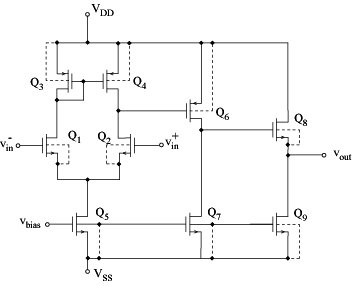
A simple CMOS implementation of the general structure:
Q1 to Q5 ... Differential stage with a single ended output (Q5 simple current source) Q6, Q7 ... Second gain stage and level shifter (Q6 driver device, Q7 load) Q8, Q9 ... Output buffer (source follower, Q8 driver device, Q9 load) Low-frequency gain of the differential stage:
l ... load parameter Q1 and Q2 are supposed to be matched Q3 and Q4 are supposed to be matched Low-frequency gain of the inverter:
Overall voltage gain:
Av = Av1 Av2 For typical biasing conditions and device geometries:
Av ~ 10 000 to 20 000
|
 Analogue filter


 i ... input parameter