 |
|
||
|
Frequency response of MOS amplifiers
For high frequency signals
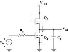
No negligible admittances of parasitic capacitances Gains and input and output impedances are functions of signal frequency High-frequency small-signal equivalent circuit of a MOSFET must be used NMOS single-ended amplifier with enhancement-mode load device
Using the high-frequency small-signal equivalent circuit the Miller effect will be taken into account Simplified equivalent circuit of MOS gain stage valid in high frequency range:
Corresponding transfer function:
Positive real zero:
sz = gm1 / Cgd1
Negative poles:
sp1 = -Gs / Cin sp2 = -GLeq / (CLeq + Cgd1) Frequency response:
By replacing s by jw
if |sp1| << |sp2| and sz :
3 dB frequency (where Av(jw) = 1/2)
w3dB ~ |sp1| = Gs / Cin If high gain is required:
|
 Analogue filter


