 |
|
||
|
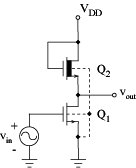
Depletion-load NMOS gain stage
Improved performance comparing to the enhancement-load gain stage
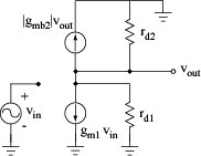
Small-signal equivalent circuit:
Current law applied to the output node gives:
Voltage gain:
Denominator of the preceding expression is much smaller than that in the case of the enhancement-load gain stage - voltage gain can be much larger Gains over 100 are possible if the substrate of the load device is separated from that of Q1 (gmb2 = 0) Both gain stages are affected by Miller effect that can be deduced from the approximate equivalent circuit:
Transfer function:
Cin ... input capacity
Result:
Capacitor Cgd1 behaves like a capacitance (1+|Av0|) times its real size ... Miller effect High-frequency gain seriously affected, bandwidth reduced
|
 Analogue filter


