 |
|
||
|
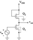
Resistor RL used in the simple gain stage is undesirable in IC realisation Usually replaced by a second MOSFET NMOS enhancement-mode device used in the Figure as Q2 Q2 is in the saturation - ensured by the short connection between drain and gate Q2 behaves like a resistor of value:
Voltage gain:
If the body effect is small (
Disadvantages: Large gain can only be obtained if the "aspect ratio" of Q1 is much larger than that of Q2 This requires large silicon area Reduced dynamic range (vout < VDD - VT must be satisfied in order to keep the load device conducting)
|
 Analogue filter


 ):
): 