 |
|
||
|
DC voltage source
Two voltage supplies available (VDD > 0; VSS ≤0) Voltages Vi where VSS < VBias < VDD can be obtained by voltage division
Seldom used in MOS technology
Output voltage (no charge impedance)
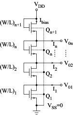
n-channel transistor in saturation VSS = 0 "Totem-pole" configuration
Voltages V01, V02, ... , V0n in the range from 0 to VDD
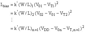
For all devices: vGS = vDS The condition for saturation vDS > vGS - VT is thus satisfied Drain current:
Disadvantage: All voltages and currents depend on the supply voltages VDD and VSS.
Depletion-mode device Q2 acts as current source Q1 is forced to carry the drain current Ibias Bias voltage V01 is thus stabilised Only one bias voltage
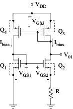
Transistors Q3 and Q4 are matched Equal currents Ibias independent of VDD Equal Bias voltage V01 independent of VDD
|
 Analogue filter


