 |
|
||
|
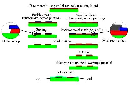
Technology of single-sided printed wiring boards For single-sided boards the simple masking and etching technique can be used. Starting with a copper clad laminate, the pattern of the wiring is screen printed onto the surface as a positive mask. Alternatively photoresist technology can also be used to make the same mask, but the much cheaper screen printing is sufficiently good for the rough resolution of common single-sided boards. From the uncovered places the copper foil is removed by etching, then the mask layer is stripped, and in the last step the holes are drilled. Masking and etching sequence for single-sided PWBs using positive or negative mask
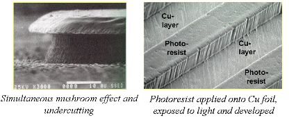
SEM photos show undercutting, the mushroom effect and photoresist application
When the pattern is ready, two types of layer are usually applied to the board surface. Solder resist mask (that is a mask resistant to soldering), which is a heat-resistant coating applied to selected areas of a PWB to prevent the deposition of solder upon those areas during subsequent soldering, and in particular to prevent solder bridging between conductive tracks. In addition, the solder resist mask is applied to improve corrosion resistance and the overall appearance of the board. With the requirement of finer and finer interconnection geometries, it is advantageous to apply the solder resist mask over all parts of the board except where solder joints are to be made. Surface finish, which is a solderable coating applied to all areas of the copper pattern, i.e. to soldering pads, where component leads are to be soldered. Solderable surface finishes protect the copper against environmental effects and humidity, thus improve solderability, in particular wetting, and consequently the electrical performance of the solder joints. Surface finishes for improving solderability
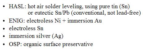
An obvious material for surface finish is tin (Sn), or eutectic tin-lead (Sn-Pb) in case of conventional – but more and more prohibited – soldering. It is cheap, easily applicable and compatible with the applied solders. An easy way to apply tin surface finish to the PWB pads is HASL (Hot Air Solder Leveling) technology, in which the substrate is cleaned, treated with flux and dipped into a solder bath. The excess solder is removed by air knives. The main disadvantage of HASL technology is that it makes the surface bumpy which is not suitable for fine pitch components. Pure tin (Sn) surface finish can be applied by immersion technology as well. If we apply pure immersion Sn, the copper pads have to be activated with special chemicals. Then the board is dipped into an electrolyte and the copper surfaces will be coated by pure Sn. Ni-Au finish is considered the best quality but not the lower cost surface finish. The nickel layer is applied by electroless and the gold layer by immersion technology, this is why this structure is called ENIG (Electroless Nickel Immersion Gold). Nickel layer gives a barrier to prevent the reaction between molten solder and copper. If we use lead-free solders, this is very important because lead-free solders form brittle intermetallic compounds with copper. ENIG technology is frequently used when besides good solder joint good thermosonic or ultrasonic wire bonding is requested too on a PWB. OSP (Organic Surface Preservative) finishes use three types of materials, as follows: benzotriazol, substitutional benzimidazol, or imidazol. The coating technology is similar to the immersion process. OSP finishes are becoming more and more popular, because they have a lot of advantages: they are fully environment sound (usually water based), very cheap, have smooth surface, are flexible therefore endurable to mechanical stresses, do not contaminate the board under application, and do not form brittle intermetallic compounds. There are two disadvantages that might prevent the application of OSP finishes: they are insulating, therefore electrical measurements by probing are impossible, and their properties degrade during reflow soldering, consequently soldering to the other side of the board encounters difficulties. Immersion silver (Ag) surface finish produces a quality similar to OSP and immersion tin, but eliminates their disadvantages. Silver becomes oxidized easily so it should be combined a kind of organic layer. Silver is suitable for wire bonding too, however, it does not reach the quality of Ni-Au, but it has much lower cost. A quite different kind of surface finish is necessary to the contact fingers of the PWB pattern. The highly conductive, mechanically hard and wear resistant layers usually applied by selective electroplating. The contact finger must be free of oxidation and corrosion and remain so for the expected life of the equipment. These requirements are generally satisfied by using electroplated nickel and gold layer structure. The nickel layer is necessary to prevent copper to diffuse into the gold. Contact fingers are plated after the PWB has been pattern plated, the resist stripped, and the copper foil etched off the laminate. The general procedure is as follows: 1. Tape circuit to expose contact fingers and prevent other parts if needed. 2. Strip tin metal etch resist. 3. Scrub the bare copper. 4. Plate nickel. 5. Plate gold. 6. Remove tape from PWB. The thickness of the nickel is usually a few micrometer, while that of the gold is less than 1 micrometer. Unfortunately the thickness of gold at the edges of the row of contact fingers can achieve 2...3 micrometers. In order to lower cost by the gold savings, it is very important to improve the distribution of the electroplated gold layer.
|
 PWB Types and Materials