 |
|
||
|
Chemical
technologies of PWBs The
chemical technologies include the cleaning, layer deposition, layer removal,
surface finishing and rinsing processes. The
most important electrochemical and electroless layer deposition processes are
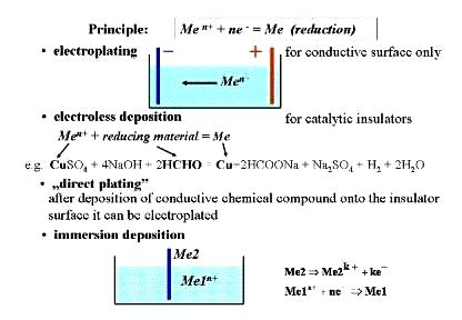
based on the same principle as shown in the figure below. Principle
of electrochemical and electroless layer deposition How to
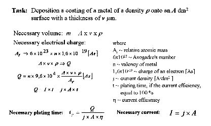
determine the technological parameters of
electroplating?
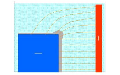
Resulting
metal thickness distribution depends on current
density
The
purpose of the electroless copper deposition
process is to metallize the isolating wall of driller holes. This metallization
provides an electrical connection between the sides of a panel, and to the inner
layers of multilayer boards. Before
electroless copper process, the drilled PWB is mechanically and chemically
cleaned by scrubbing, removing of grease, micro-etching and oxide-removing.
Then the
surface of the PWB must be activated. Activating is necessary, because the
copper coating must be deposited onto the isolating surface of epoxy-resin.
After this stage PWB is ready to metallization, which usually means through-hole
plating. The
electroless copper deposition process is based on the chemical reduction of
copper initialized by the activating particles. Slow operating type of
electroless copper bath is used to deposit a very thin, but continuous layer of
copper. Electroless copper layers, deposited from a room temperature bath, are
only ca 1 micrometer thick. The advantage of this type of bath is the careless
operation. When using slow operating type of electroless copper bath, the thin
coating of electroless copper is thickened by electroplating. In this way the
copper coating being inside the holes is formed by a two-stage depositing
process: electroless copper followed by electroplating. By using quick
operating electroless copper bath, it is possible to deposit the copper
coating by a single-stage process, without electroplating. When panels are
removed from the electroless copper bath, they should be neutralized, rinsed,
dried as soon as possible to prevent oxidation. Panels are typically dried
during a mild scrubbing operation. When
inspecting panels as they are being processed along the electroless copper
line, attention must be paid to the holes, not just the surface of the board.
The surface may appear satisfactory, while little coverage is taking place
inside the holes or along the edges. Panel edges are a more accurate reflection
of copper deposition quality inside the holes, than the surface is. If there is
a marginal condition in the electroless copper process, it will show up inside
the holes first, then on the board edges, and lastly on the
surface. The
dwell time in copper is usually 15-20 minutes. Electroless copper is a solution
containing sodium hydroxide also. This component is hygroscopic, which means
that it will pull moisture out of the air. Caustic solutions like electroless
copper baths are difficult to rinse off. The only fully reliable way to rinse is
to neutralize first, then rinse. Usually 1% solution of sulfuric acid or
phosphoric acid is used for neutralizing. In the course of an operating shift,
analysis should be conducted, involving pH check of the all copper baths.
Most of
the baths require an air source which pumps bubbles through the bath at all
times. The air is beneficial for two reasons: air helps stabilize the copper and
retard any tendency to plate out; and air provides a small measure of solution
agitation when the tank is not being used. During use, there is plenty of
agitation by way of moving of panels, or by a mechanical rack agitation system.
It should be remembered, that only a trickle of air is required for good bath
stability: too much air agitation removes the formaldehyde (which will
extinguish the deposition reaction). According
to the imaging, electroless copper process can be followed by
electroplating. Electroplated copper thickness is ca 5 micrometers. This
panel plating is necessary, when PWB is microetched before pattern plating. Microetching means
removing of ca 2-3 micrometers thick layer of copper. PWB
plating system for electroless deposition and pattern
plating The
copper surface of the PWBs must be cleaned and then a negative mask is made onto
the surface of the PWB, after electroless copper process and prior to pattern
plating. There
are differences in the cleaning processes which
must be used for photoresist imaging and screen printing. Dry photoresist filmed
panels require microetching of the copper surface prior to electroplating.
If this is neglected, all copper would peel. The copper surface must be etched
until it is matte pink. For screening resists the type of the cleaner depends on
the solvent of the resist. After
through-hole plating and prior to panel plating a negative mask should be
applied to the board surface. The aim of the negative mask is to form a
selective covering on the copper surface according to the layout of the circuit.
Negative masking means, that the required pattern of the PWB is not covered by
resist. The mask formed before pattern plating must be resistive against plating
baths. For patterning (or imaging) with negative mask, the dry film photoresist method is the most
popular in the PWB industry. Alternatively, the less expensive but lower
resolution screen printing imaging
technology can be used. Both processes are discussed in the next
page. The
purpose of pattern plating is to
deposit ca 25 micrometer thick copper onto the wall of the holes. The copper is
coated by tin or tin-lead by electroplating. The thickness of this coating is ca
10 micrometers, and it serves as a mask during etching, and called metal etch
resist. In plain cases it can be used as a solderable coating when assembling
and soldering components onto the board. Some chemicals (brighteners etc.) must
be added continuously to copper plating and other baths. All plating baths have
a certain degree of tolerance for organic and metallic contamination, and for
components. Pattern
plating is followed by stripping, i.e. removing the negative photoresist mask
and etching the copper. During this process the tin coating will protect the PWB
circuitry against the etchant. Etching is the
process, which actually transforms an image into a circuit. In general,
conveyorized alkaline ammonia or sulfuric acid/hydrogen peroxide baths are used
for etching. Processing
line for etching after negative mask stripping Organic
resists are formulated to withstand most etching solutions. They all withstand
common acid etchant. Alkaline soluble screen printing inks are not formulated to
work well in etchants with pH above 7.5. Vinyl screen printing resist, and
solvent or semi-aqueous developing dry film photoresist work very well as etch
resist. The fully aqueous developing photoresists should be given more
careful consideration, and therefore most commonly used for plating resist, and
tin metal etch resist technology is preferred. The
etching rate can be defined as the etching through time of a 35 µm thick copper
layer. As the copper foil is etched, some amount of copper is also removed from
the sidewalls of the conductors with a lower etching rate. It is the so called
undercutting. Undercut depends on etching technology, etchant, pH, etc. A
high etch factor, which means low overhang, generally indicates the ability to
hold fine lines with tight conductor spacing. Excessive overhang causes short
circuiting, as the overhanging conductor breaks off and forms an electrical
bridge between two points in the circuitry. Overhang can be eliminated by fusing
(or reflow) of tin metal etch mask. Using
thin copper foils on the laminate can be very helpful in reducing undercutting,
attaining fine lines with high density and in using differential etching
for bare copper circuitry. Differential etching occurs when the plated copper is
used as the etch resist. To do this, the plated copper must be considerably
thicker than the copper foil. Tin
metal etch resist stripping by selective etching
|
 PWB Types and Materials