 |
|
||
|
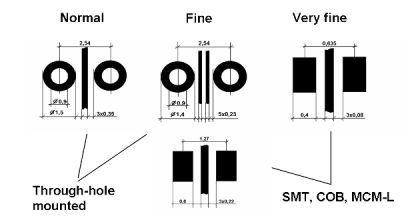
PWB types according to pattern resolution and vias The applicability of a printed wiring board, and, as a consequence, the quality of its conductive pattern can be characterized by the minimal width and spacing of conductive lines, which value is also called resolution. The quality of the pattern and the resolution can also be characterized on the basis of a typical pattern part around two holes next to each other (see the figure below). In a normal (or conventional) configuration the distance between these holes is the usual 2.54 mm (2.54 mm = 1/10 inch). For normal patterns the typical value of the line width and spacing is 0.3 mm or higher, and it is the same for the width of the ring around the hole. If the diameter of the hole is 0.9 mm, there is space only for a single track line between the holes. For fine patterns the typical line width is around 0.2 mm and if the hole diameter is the same 0.9 mm, two lines can be conducted between two holes. For very fine patterns the resolution is less than 0.1 mm, and the hole diameter can be 0.3 mm or less, if necessary, so more than two conductive lines can be placed between the holes. Printed wiring boards with fine and very fine pattern resolutions, however, are more frequently used for surface mounting technology (SMT), therefore the characteristic resolution patterns are from SMT boards. Normal, fine and very fine conductive pattern parts
Nonmetallized holes with round, rectangular or any other shape are used for fixing components onto the board either by inserting the component leads through them or by using surface mounting technology (SMT) or chip-on-board (COB) assembling methods. The metallized holes are used not only for through-hole assembling the components, but for producing interconnections between the tracks of different conductive layers. Vias are not intended to insert component leads into them, they are only interconnections, electrically or thermally joining different conductive layers of a multilayer structure (see figure below). A through-board via connects both outer layers and, not necessarily, inner layer(s). A blind via connects an outer layer and at least one inner layer, but does not connect both outer layers. A buried via makes interconnection between only inner layers of the board. The aim of a thermal via is to conduct heat from a component heat source to a heat sink layer of the structure. Examples of vias and the aim of through-hole metallization 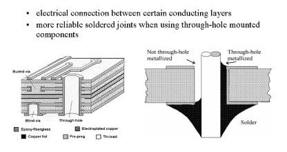 In order to interconnect the printed board with the other boards and components of the system, a set of wires, cable(s), or backpanel(s) are connected to the conductive pattern of the board, using connectors to get nonpermanent contacts or solder joints to get permanent contacts. A connector is a device used to provide mechanical connect/disconnect service for electrical termination. An indirect connector has two parts: one, whose set of contacts are mechanically and electrically attached to the printed board, and the other, which mates with the first part of the connector, and whose contacts are attached to a set of wires, a cable, or a backpanel. An edge-board connector can replace the second part of the connector, if edge-board contacts are printed on or near any edge of the printed board for mating this edge-board connector. Connector tang is the name of that portion of a printed board which contains printed contact fingers, and mates with an edge-board connector. When none of these connector types is used, the interconnecting wires are usually soldered to the printed soldering pads formed on the connector area of the board. In general meaning, a backpanel or backplane is an interconnection device used to provide point-to-point electrical interconnections. It is usually a printed board that is assembled with discrete wiring terminals on one side and connectors on the other side. Mother board is the name of a similar printed board assembly, which is used for interconnecting arrays of plug-in electronic modules.
|
 PWB Types and Materials