 |
|
||
|
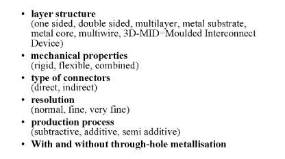
Types of printed wiring boards A printed wiring board (PWB) is a substrate, which is made up of an insulating board with copper foil tracks on its outer surfaces. At the single-sided PWBs, copper foil wiring tracks are on one of the outer surfaces only. More and more frequently multilayer PWBs are also in use, where wiring tracks are fabricated in the form of inner layers as well. When speaking about printed wiring boards, it is always necessary to keep in mind that when the board is ready discrete components are assembled to the board. The components are usually fixed to the PWB and connected to the conductive copper tracks by soldering. Sometimes the chip-on-board technology is used for the assembly of semiconductor chip components: integrated circuit chips are attached directly to the board using adhesives and the electrical connections between the contact pads of the chip and the board are made by micro scale wire bonding (chip-and-wire technology). The final assembly is named printed circuit (PC), PC card, or surface mounted assembly (SMA). The main aspects and groups for selecting and categorizing PWBs are as follows: - number of conductive layers: single-sided, double-sided, or multilayer; - rigidity of the insulating board: rigid, flexible, or combined (rigid-flex); - type of connectors, namely PWBs with direct (edge-board) or indirect connectors, or applying no connector; - quality of the conductive pattern: rough, fine, or very fine; - characteristics of the production, e.g. subtractive or additive, semiadditive, metal core, PWBs with embedded passives, etc.; - type of holes: nonmetallized holes, plated-through holes, or vias (including through-board, blind, and buried vias). Aspects of grouping and the main types of PWBs
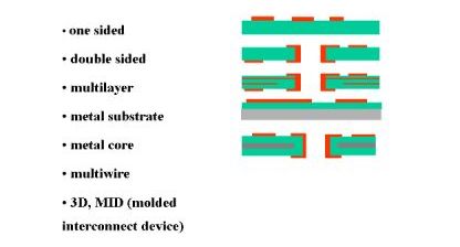
The single-sided boards have only one patterned conductive layer, and are used for very simple applications. Nowadays the double-sided PWBs are the most widespread, where there are two conductive layers in the laminate, on the two outer sides of the board. The tracks formed from the two conductive layers are interconnected where necessary by plated-through, i.e. metallized holes. The components are usually assembled onto the board by the insertion of their leads through the same holes. This process is called through-hole assembly. If surface mounting technology (SMT) is used, where components are assembled onto the surface of the board without the insertion of the leads into the holes, the holes only serve as interconnections, they are usually produced with smaller diameters and called vias. Multilayer printed wiring boards contain more than two, typically four conductive layers. Since there are a significant decrease in the average size of components and an increase of the component density on the cards, the need for and the production of the multilayer printed wiring boards are going up. PWB categories according to the layer structure
|
 PWB Types and Materials