 |
|
||
|
Design the interconnection pattern and the package of the circuit
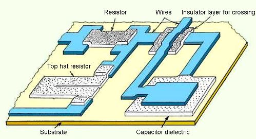
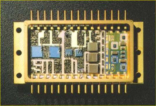
When all the elements are designed, their placement and the routing of the interconnections are to be carried out. The conductive pattern on the substrate contains the footprints needed for mounting the components and for the interconnection routes. The mounting and joining processes of hybrid components are determined by their types. For semiconductor chips the chip-and-wire technology can be used. The chip can be attached to the substrate either by eutectic soldering or using conductive adhesive. The former process needs a screen-printed gold underlayer, specific equipment and technique, and it provides a better but more expensive joint than conductive gluing. The electrical connections between the chip and the properly placed pads are produced by thermocompression or ultrasonic wire bonding applying thin gold or aluminium wire. A thick film circuit using flip-chip and other hybrid components
Surface mounting devices can be placed to the substrate of a hybrid circuit applying the same pick-and-place machines, which are used for SMAs. Before placing the components, the contact pads should be presoldered either by dip soldering or by screen-printing solder paste. The package design of a power hybrid circuit
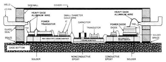
The placed components are attached to the conductive pattern by reflow soldering. Since the substrate has good thermal conductivity, the heat, which is necessary for remelting the solder, can be provided through the substrate, conveying or simply placing the assembly onto a heated plate. The lead terminations of the circuit are also soldered to the pads along the edges of the substrate in the same process or by applying dip soldering. Encapsulating the package is the last step in the technology. There are many approaches of packaging, and hybrid integrated circuits adapt to all kinds of it, from inexpensive plastic and ceramic packages to the expensive and highly reliable metal-glass package. After packaging, the circuits are finished by functional testing and marking. A thick film circuit in a premolded plastic package
A thick film circuit assembled into a hermetic metal-glass package
In the following it is summarized how to obtain the masks, which are necessary for the fabrication of a hybrid circuit, starting from the original electronic design of the circuit. The usual design steps of a hybrid circuit are summarized as follows: - original schematic design: sketched circuit diagram, computer analysis, model with discrete components; - hybridization: analysis, design of integrated components, selection of the hybrid components, pick a package; - circuit layout design: component placement, routing; - mask generation: artwork generation and photoreduction, or direct mask generation; - prototype building; - prototype analysis: electrical and thermal analysis, quality tests; - design correction if necessary. The original schematic design can start in many forms. Probably the most common sequence is to begin with a circuit diagram and then progress to a 'prove-out' stage with a computer analysis and with building and testing a model using discrete components. In every step it should be kept in mind that the task of the hybrid circuit designer is to design a hybrid that will replace the discrete version. In the course of hybridization an important task of the hybrid designer is to pick the package for the circuit. The package naturally must be larger enough to get all the individual elements into it and to dissipate heat that will be generated. At the same time, if it is too large, the advantage of compactness will be lost, as well as the advantage of low cost. The circuit layout design is critical. It is a complex process, best done by designers who know what they are doing. Doing it over and over again is very helpful. Experience pays. It is very important to view the thick film layout as a circuit diagram; or to view a circuit diagram as the basic thick film layout pattern. Because of this, the first step in the layout design process is to change the original circuit diagram to a topographic layout. The package-picking and size-predicting step needs assignments of proper area to each component. In the case of surface mounting components this assignment is based on the footprint, which is the area of the component plus the area needed for the pads to which the component will be attached. In general, a specific power of p= 50mW/mm2 for thick film resistors is used, and A, the area of the resistor, is estimated from the power of the resistor P by the formula A = P/p. For avoiding very small resistors a minimum limit of about some tenths of mm is used. Space must also be allocated to lead pads and for white space between components. If an integrated capacitor will be used, its area can be calculated from the net area needed for the capacitance plus the area of the border around it. From the areas of each component and the spaces, a tentative total area can be computed. The total power dissipation in the circuit can be also calculated. These two estimated figures, the total area and the total power dissipation, are all that is required to pick a package, along with knowing how many leads will be needed. A common rule of thumb is that total heat generated is to be limited to 1.5 W for a Once the layout of the circuit is completed, the next task is to generate the masks. Computer Aided Design technique and automatic mask generation are wide-spread for generating masks. Specially packaged, surface mounting active devices are now very widely used in professional thick film hybrids. Some passive components, e.g. surface mounted ceramic chip capacitors, are also compatible in size and have some advantages over the printed elements (e.g. higher capacity/volume due to multilayer structures), so their application is preferred. The other elements, viz. resistors, low value capacitors and conductors are produced as thick films. Finally, the following collection of layout rules summarizes the experience of the designers, reflects to the limitations of the materials being used, and partly it is the result of the application of simple common sense. The rules are grouped in accordance with the design of conductors, pads and crossovers. Sometimes the term resolution is used, which is the synonym of and equal to the minimum line width and spacing determined by the applied technology. Note, that when hybrid technology applies surface mounting, the design rules of SMAs should be taken into consideration. 1. Avoid long and narrow conductor lines, because they may have high resistance. For thick film hybrids 2. Solder bonding pads for wire leads should be at least three times wider and longer than the wire diameter. Narrow and short pads result in leads that peel off easily. Bonding pads for soldering surface mounting chip components should be larger, at least by the resolution, than the dimensions of the component. Pads for semiconductor chips should be designed with at least an 0.1mm border on each side. Wire bonding pads should be at least 3. Avoid crossovers. Sometimes crossovers can be eliminated by running conductors between the connection pads of a surface mounted component. To avoid a short it is advisable to cover the conductor under the component with a protective solder resist layer. Crossovers can be replaced by jumping over conductors with bonding wires going from a chip to any of the connection pads, or between two extra connection pads. It is necessary to protect the integrated elements and conductors over which the lead passes. Sometimes it is possible to avoid crossovers by using the back side of the substrate by going around the edge. Some packages have leads that attach to both sides of the substrate, offering automatic access to the opposite side. When all else fails, crossovers have to be placed in the circuit layout. There is really nothing wrong with this, except that it additionally needs at least an insulating and a conductive layer, which increases the price of the final circuit. The designer must also keep in mind that crossovers have parasitic capacitance.
|
 Screen Printing