 |
|
||
|
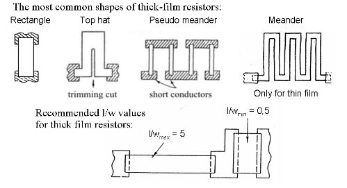
The most common shapes of integrated film resistors and the recommended l/w values
For the selection of the sheet resistance it should be taken into consideration that the ideal resistor aspect ratio is 1. To print a reasonable range of resistors with a single screen, the aspect ratio is extended to a range of about one order of magnitude, from 0.5 to 5. The effect of the resistor shape on the current density in the layer
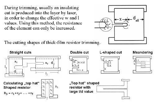
To make an even wider range of resistors without using an extra screen-printing step, this range is sometimes stretched to two orders of magnitude (i.e. from 0.2 to 20). High aspect ratios are difficult to trim. The top-hat and meander shapes are ways to achieve high aspect ratios. Meanders of very high aspect ratios are not recommended, the more suitable pseudo-meander arrangement with shorting bars can be used instead. Cutting shapes of thick film resistors for trimming
In order to obtain higher accuracy, thick film resistors are generally trimmed. The different trimming geometries which are now in use are as follows: straight cut, double cut, L-cut, meandering and top-hat. In the course of designing trimmed resistors a proper room should be left for starting the cut from the outside of the resistor area. Trimming should not begin near another resistor; otherwise trimming of one resistor can change the value of an already trimmed resistor. The trimming cuts are allowed in only the X or Y directions. 'Hot spots', i.e. places with high current density and, consequently, with high local power dissipation on the trimmed geometry, should be avoided. The power calculations should be done on the trimmed resistor geometry, and not on the untrimmed geometry. Closed loops cannot be trimmed, unless the trimming system is very sophisticated, so if the circuit contains loop, trimming must be done with the loop open. The loop can be closed later with a wire jumper, but it is not recommended for mass production. The overall place required by a resistor on the substrate contains the area of the terminations, too. Conductor termination pads for resistors should be at least 0.2 mm larger on each side than the resistor that will be printed over it. The overlapping is at least 0.3 mm. These values are mainly determined by the inaccuracy of the alignment of the screens used for subsequent printings. In this way it is ensured that the resistor makes good contact with the terminations, even when the alignment is not completely correct. When all the elements are designed, their placement and the routing of the interconnections are to be carried out.
|
 Screen Printing