 |
|
|
Introduction to Thick Film Technology
Aims
The objective of the course is to present the physical background of the processes, the fabrication sequences and the most important design rules of the integrated elements of thick film microelectronic circuits.
The objectives of this course are to:
- Understand the basic principles and tools of screen printing technology.
- Learn the properties of materials used in thick film technology, and how their structure is formed during the firing process.
- Be acquainted with the entire fabrication sequence of thick film circuits including laser trimming, component and lead soldering, as well as, encapsulating for protection.
- Understand and apply design principles for integrated resistors and the layout of thick film hybrid circuits.
Contents
The course gives an introduction to the technology of thick film hybrid microelectronic circuits, and the design of their integrated resistors and layout. The course has the following tasks:
- Screen Printing
- Firing of Thick Films
- Fabrication Steps of Thick Film Circuits
- Thick Film Circuit Design
|
|
Thick Films: Screen Printing and Firing.
The basic layer deposition and patterning processes
Thick film technology is used to create conductive, resistive and capacitive layer patterns on ceramic substrates. These thick film substrates can be used as passive integrated networks or - with the application of additional surface mounted components - as hybrid microelectronic circuit modules.
A thick film circuit
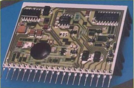
The technology is termed 'thick film' because the layers are deposited by screen-printing and firing, and they have the thickness of 5-50 micrometer, ten to hundred times thicker than that of the films produced by vapor deposition or sputtering and called 'thin films'. The miniaturized thick film components and networks provide high power dissipation and excellent reliability coupled with high automation of the manufacturing process. |
|
|
|
 Task 1: Screen Printing Task 1: Screen Printing
The aim of this task is to learn the screen printing process, which is the principal step of thick film technology for layer deposition and patterning.
The screen printing process is followed by settling, drying and firing. While screen printing determines the pattern of the thick film layer, firing creates the structure of the layer and - as a consequence - determines the properties of the thick film components.
Since a thick film circuit is usually a multilayer structure, its fabrication needs several printing and firing processes, one after the other.
Contents:
- Screen printing: the characteristic layer deposition and patterning process of thick film circuits
- Screen mask: the patterning tool tool for screen printing
- Types of screen masks:
1.) emulsion masks and
2.) metal masks
Task 2: Firing of Thick Films The aim of this task is to learn the basic properties of thick film materials and the principle of the firing process, which fabrication step creates the layer structure and - as a consequence, together with the materials characteristics - defines the properties of the thick film components.
The firing process is preceded by the screen printing of the layer. Screen printing determines the pattern of the thick film layer, and firing creates its final materials structure.
Since a thick film circuit is usually a multilayer structure, its fabrication needs several printing and firing processes, one after the other.
Contents:
- Thick film materials: substrates; conductive, resistive and dielectric layers
- The firing furnace
- The firing process: the temperature profile, and its drying, firing and annealing phases
Task 3: Fabrication Steps of Thick Fim Circuits The aim of this task is to learn the basic fabrication processes of thick film hybrid circuits, going through the technology step by step.
The technology of thick-film substrates for passive networks and hybrid circuits is based on an additive process: the various layers and their patterns are formed by screen printing in the same step.
Screen printing is followed by leveling, drying and firing/burning. The structure of the layer and all of its essential properties are formed during firing. When two subsequent printed layers are not overlapping, their firing can be done in the same step.
Since a thick film circuit is usually a multilayer structure, its fabrication needs several printing and firing processes, one after the other.
Further important processing steps of the production of thick-film hybrid IC-s are as follows: trimming, mounting, encapsulation and packaging to an electronic circuit module or system.
Contents:
1. Thick film circuit fabrication step by step:
- Screen printing and firing a conductor layer onto a ceramic substrate;
- Screen printing and drying various resistor layers and firing them in a single step;
- Laser trimming of resistors;
- Solder mask printing and firing;
- Solder paste printing;
- Mounting components;
- Reflow soldering.
2. Laser trimming of resistors:
- Trimming technologies, laser trimming of thick film resistors;
- Schematic structure of a laser trimming system;
- Laser system for trimming and marking.
3. Main parameters of cermet and polymer thick-film resistors.
Task 4: Thick Film Circuit Design The aim of this task is to learn the basic design rules of thick film hybrid circuits, especially of thick film integrated resistors.
The technology of thick-film substrates for passive networks and hybrid circuits is based on an additive process: the various layers and their patterns are formed by screen printing in the same step. Screen printing is followed by leveling, drying and firing/burning. The structure of the layer and all of its essential properties are formed during firing. Both the pattern and the properties of the thick film integrated components are influenced by the laser trimming of resistors.
When designing a thick film integrated circuit, in particular its integrated resistors, in addition to determine the layout to meet the electrical requirements of the circuit, it should be taken into consideration that the layout will be realized by using the screen printing and laser trimming processes.
Subsequent processing steps, which should be considered as well, are as follows: assembling, soldering, encapsulation and the final mounting of the circuit module to an electronic system.
Contents:
- Design rules and shapes of integrated thick film resistors;
- Design of the resistor elements;
- The most common shapes of integrated film resistors and the recommended l/w aspect ratio values;
- Typical laser cutting shapes for thick film resistor trimming
|
|
|
|

 Screen Printing