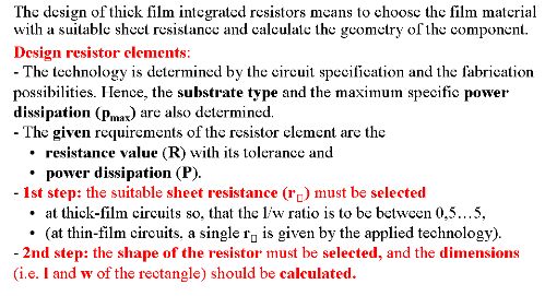
|
|
||
|
In the simplest case, the design of a resistor element means to choose the proper film materials for the resistors and determine their surface geometry. Design of the resistors should be preceded by the selection of the conductor paste. The type of the applied conductor paste is selected on the basis of the sheet resistance, solderability, line resolution, adhesion to the substrate, metal migration characteristics and bondability. The sheet resistance of conductor pastes falls in the range of 2 - 150 mohm, depending on the material of the conductive constituent. Ag/Pd metal alloy pastes with 15 - 60 mohm are the most widely used for resistor networks and for solderable interconnection patterns. Gold (Au) pastes with 3 - 5 mohm sheet resistance are used for thermocompression wire bonding, eutectic die soldering and in high reliability applications. Other precious metal pastes are used for special applications, such as multilayer interconnections or temperature sensors. In the case of resistor pastes, the main characteristics are the desired resistance range, sensitivity to temperature and moisture, the allowable power dissipation, stability and so on. Sheet resistance values of resistor pastes are now available in decimal increments from 0.1 ohm to 100 Mohm. Intermediate values may be obtained by means of blending pastes from the same resistor system. The layouts of all printed layers are usually designed with the help of a computer, applying CAD (Computer Aided Design) systems.
|
 Screen Printing