 |
|
||
|
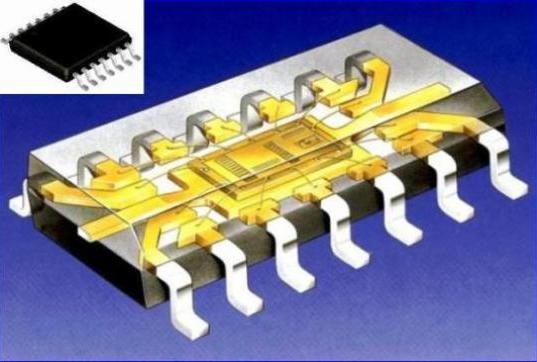
The animated figure above shows the most important steps of the fabrication of a typical thick film hybrid integrated circuit (IC). In thick film technology ceramics substrates are in use. Substrates provide base onto which all thick film elements are screen printed and fired, therefore they influence on the electrical and thermal performance of the circuits. The most widely used substrates are alumina (Al2O3) ceramics, consisting of 94 - 96 % Al2O3 and providing very good adhesion to the fired layers. Pastes applied in thick film technology are colloidal systems. They have three main components, as follows: 1. The powder of the functional phase. - Conductor pastes are manufactured using powders of precious metals such as Ag, Pd, Pt and Au, or their alloys. Most widely used composition is Ag‑Pd. To increase the conductivity, copper-based pastes are also in use; however, they should be fired in neutral atmosphere (generally in high-purity nitrogen) to avoid the oxidization of non-noble metal particles. The conductor pastes are used to prepare the conductor network, the mounting pads and the external lead pads as well. - In case of resistors the functional phase consists of metals or oxides. Nowadays ruthenium-based resistor systems are applied. The principal versions of them consist of ruthenium-dioxide (RuO2) and/or bismuth-ruthenate (Bi2Ru2O7). Ruthenium-based resistor systems have low temperature coefficient (TCR: +-50 - 100 ppm/deg C) and good stability (lower than +-0.1 - 0.5 % after 1000 hours storage at 150 deg C). - The functional phase for high-dielectric-constant capacitor dielectrics is some type of ferroelectric ceramic powder e.g. barium titanate (BaTiO3), while in case of low-dielectric-constant insulators - applied for preparation crossovers or multilayer systems - they are glass or glass-ceramic powders. 2. The second main component is finely divided vitreous nonconductive binder. A firm bonding between the metal and the substrate is obtained using low melting point glass powder and/or metal oxides, mixed into the pastes. On firing, the individual grains of the dispersed glass melt, thus forming a matrix structure in which the metal grains are lodged to form conductive chains. In addition, the molten glass wets the surface of the substrate and flows into any small surface irregularities, so that on cooling, good adhesion between the metal layer and the ceramic is ensured. The metal oxides of the glass also react chemically with the substrate material that causes further improvement of adhesion. 3. The third component is called vehicle. It is an organic system, which gives the desired printing characteristics, since the powder mixture is intended to be screen-printed, the pastes must be manufactured to show certain rheological properties. Laser trimming is the next processing step in thick film technology. Components (usually resistors), as printed and fired, have distribution of their values too far from the desired value to be used for some application. The corrective process is called trimming. The most common method to trim thick film resistors are to change their surface geometry preparing a cut into the layer. The cut reduces the cross-sectional area and increases the mean length of current path, so it increases the resistance value. The most widely used material removal technique is the laser trimming. Applying this technique, high precision components (< 0.1 %) can be manufactured. Solder mask or solder resist layer is applied to avoid short-circuits, to improve the quality of soldered joints, and to give protection and better appearance of the circuit. Generally screen-printed and fired, low melting point glass layers are used in thick film hybrids as solder resist masks. Solder paste is applied onto the mounting pads of the thick film circuit before component mounting. The solder paste is deposited either by screen printing for high volume production or by syringe dispensing in the case of low volume and prototype fabrication. As an alternative, the contact pads can be presoldered by dip soldering before placing the components. The composition of solder pastes differs basically from resistor or conductor inks since in solder pastes the powder of solder, e.g., tin-lead (SnPb) or lead-free alloy, and fluxes are mixed with organic binder. By the use of solder pastes, fluxes and solder material can be applied simultaneously to the desired part of the circuit. Mounting components means the application of Surface Mount Technology (SMT), which is also very popular for assembling printed circuit boards. SMT is the method in which the specially encased components, called Surface Mounted Devices (SMD) are attached to the mounting pads on the thick film substrate. After mounting, the SMDs are fixed by soldering. The most widely used SMD-s, such as resistors, capacitors, discrete semiconductor devices and IC-s, have a very wide selection. In mass production highly automated mount equipment are in use. The most popular pick-and-place systems apply a placer head that one after another picks up and fits components onto the substrate. Small outline integrated circuit (SOIC): outside and inside
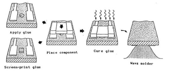
- using wave soldering; components should be stuck by special adhesive, - applying reflow soldering; components with small and medium sizes are sufficiently fixed by the sticky solder paste, but heavy components have to be stuck by adhesive. Assembly steps of surface mounting technology (SMT) using wave soldering
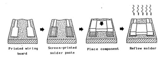
Assembly steps of surface mounting technology (SMT) using reflow soldering
Reflow soldering is usually used after mounting to fuse the screen printed solder paste layer and fix the components to the soldering pads. One possibility to heat up the solder paste is the usage of infrared furnace with air, or with neutral gas (typically nitrogen) atmosphere. The first phase of the reflow soldering process is the preheat of the circuit up to ca 130 deg C. For melting the solder paste, high rate heating above the melting temperature of the solder (ca 225 deg C for SnPb, and 260 deg C for lead-free solders) is applied. Finishing the soldering process the rest of flux is removed from the circuit by cleaning, unless solder paste with no-clean flux is used. Infrared (IR) reflow soldering oven and the temperature profile
Pick-and-place and reflow soldering in infrared (IR) oven
Pick-and-place and reflow soldering on a belt fed hot plate
|
 Screen Printing


