|
|
||
|
screen printing and firing of various paste materials
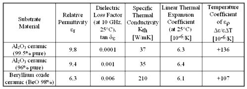
The principal steps of thick film technology are screen printing of pastes onto ceramic substrates and - after leveling and drying - firing them at a typical temperature of 850 deg C. This fabrication step creates the layer structure and - as a consequence, together with the materials characteristics - firing defines the properties of the thick film components. In thick film technology ceramics substrates are in use. Substrates provide base onto which all thick film elements are screen printed and fired, therefore they influence on the electrical and thermal performance of the circuits. The most widely used substrates are alumina (Al2O3) ceramics, consisting of 94 - 96 % Al2O3 and providing very good adhesion to the fired layers. Thermal conductivity of substrates is one of the most important design parameter, due to the frequent requirement for maximum heat dissipation from thick film circuits. For circuits of very high dissipation beryllia (BeO) or AlN substrates are in use, due to their thermal conductivity is about 12 times higher than that of alumina, although their production cost is also much higher comparing to the alumina substrates. The most important substrate properties can be summarized as follows: - Dimensional stability - High electrical resistance - High thermal conductivity - Good adhesion of the layers - Thermal compatibility with components - Low dielectric constant (not satisfied in alumina) - Low dielectric loss tangent - Low price Properties of substrate materials
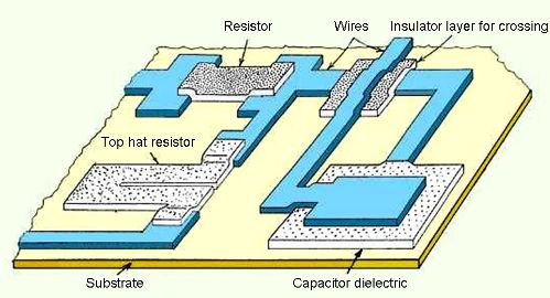
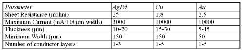
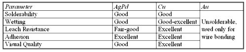
A wide variety of pastes is available to suit different application and requirements. Pastes are classified in accordance with their functions into three groups: conductor, resistor and dielectric pastes. The pastes are colloidal systems that become ceramic like composite layers as the result of high temperature firing. Thick film pastes are colloidal systems with three main components, as follows: - the powder of the functional phase, which is made of: metals (e.g. Ag-Pd or Au) for conductors; metals or oxides (e.g. RuO2) for resistors; titanates (e.g. BaTiO3) for insulators of high dielectric constant; and glass or glass-ceramic powders for insulators of low dielectric constant, applied for preparation crossovers or multilayer systems, - nonconductive binders, usually low-melting-temperature glass frits, and - an organic system, mainly solvents, which gives the desired printing characteristics. The materials of the three main components are detailed in the followings: 1. The powder of the functional phase Conductor pastes Conductor pastes are manufactured using powders of precious metals such as Ag, Pd, Pt and Au, or their alloys. These powders do not oxidize during firing in air and thus retain their good conductivity and solderability. Most widely used composition is Ag‑Pd. To increase the conductivity, copper-based pastes are also in use; however, they should be fired in neutral atmosphere (generally in high-purity nitrogen) to avoid the oxidization of non-noble metal particles. The conductor pastes are used to prepare the conductor network, the mounting pads and the external lead pads as well. Resistor pastes In the case of resistors the functional phase consists of metals or oxides. Nowadays ruthenium-based resistor systems are applied. Two principal versions of them consist of either ruthenium-dioxide (RuO2) or bismuth-ruthenate (Bi2Ru2O7). Ruthenium-based resistor systems have low temperature coefficient (TCR: +-50 - 100 ppm/deg C) and good stability (lower than +-0.1 - 0.5 % after 1000 hours storage at 150 deg C). The sheet resistance (r) is the basic parameter of resistor pastes. The definition of the sheet resistance is: R = r*l/(t*w); r = r/t; R = r*l/w; where R is the resistance of the thick film resistor having specific resistance of , layer thickness of t, resistor length of l and resistor width of w. The r value therefore refers to the resistance of a square in the conductive or resistive layer, and it is these squares which, when laid end to end, constitute the conductive or resistive line. The l/w geometric factor or aspect ratio of the layer is also called number of squares. Sheet resistance is determined by the ratio of conductive pigment to insulating glass. The pigment normally has a positive temperature coefficient (TCR), i.e. resistance increases as the temperature rises. However, depending on its chemical composition, the glass shows a highly negative TCR. Using proper composition and adding suitable modifiers, the temperature dependence of the layer can be minimized for the wide working temperature range of the circuits (-55 deg C to +125 deg C). Resistor paste suppliers offer decimal series of pastes covered wide range of sheet resistance (1 ohm - 10 Mohm). Capacitor dielectric pastes The functional phase for high-dielectric-constant capacitor dielectrics is some type of ferroelectric ceramic powder e.g. barium titanate (BaTiO3), while in the case of low-dielectric-constant insulators - applied for preparation crossovers or multilayer systems - they are glass or glass-ceramic powders with some special oxide (TiO2, Al2O3) fillers. The characteristic value of high K relative dielectric constant of dielectric pastes is among 10 and 1500, most frequently K equals to 200 or 500. Cross-over, solder resist and protective coatings Pure glass thick films of low dielectric constant are also applied as protective and solder resist layers. 2. Nonconductive binders The second main component is finely divided vitreous nonconductive binder. A firm bonding between the metal and the substrate is obtained using low melting point glass powder and/or metal oxides, mixed into the pastes. The glass frits mostly used are of the PbO×B2O3×SiO2 type, lead bismuth borosilicate (PbBiBSiO2), or oxides, like CuO or Bi2O3. On firing, the individual grains of the dispersed glass melt, thus forming a matrix structure in which the metal grains are lodged to form conductive chains. In addition, the molten glass wets the surface of the substrate and flows into any small surface irregularities, so that on cooling, good adhesion between the metal layer and the ceramic is ensured. The metal oxides of the glass also react chemically with the substrate material that causes further improvement of adhesion. 3. Organic solvents The third component is also called vehicle. It is an organic system, which gives the desired printing characteristics, since the powder mixture is intended to be screen-printed, the pastes must be manufactured to show certain rheological properties. For this reason the powders are mixed with resins, solvents, surfactants and wetting agents. Ethyl cellulose and acrylate resins are most frequently used. Alcohols such as terpinoel are used as solvents. The main requirement imposed upon these organic vehicles is that they should ensure good workability of the pastes during screen-printing and sharp contours after printing. The solvent is vaporized after printing by a drying process at a temperature of about 150 deg C. The residual resin keeps the powder mixture together and on the substrate so as to give an accurate representation of the screen mask. The most important properties of conductive thick films can be summarized as follows: - High electrical conductivity - Good adhesion to substrate - Good solderability - Good bondability - Low price Main parameters of thick film conductors
Soldering properties of thick film conductors
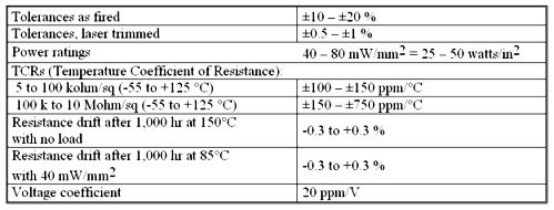
The most important properties required from thick film resistors are as follows: - Large range of resistor values (sheet resistance: 1 - 109 ohms/sq) - High stability - Low thermal coefficient of resistance - Low voltage coefficient of resistance - Low noise
Main parameters of thick film resistors
The desired properties of thick film dielectrics are the followings: - High insulation resistance - High breakdown electric field - Low dielectric constant for insulations - Suitable/high dielectric constant for capacitor - Low temperature coefficient of capacitor dielectrics - Low voltage coefficient of capacitor dielectrics - Low loss tangent - Low porosity
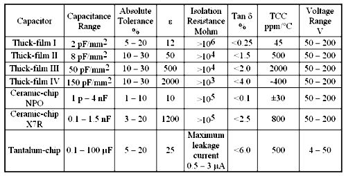
Properties of capacitors used in thick film technology
After screen printing of a paste, the deposit retains the mesh pattern for a short time; and it needs 8 - 30 minutes settling at room temperature for leveling. Then a drying process, at 100 - 150 deg C for 15 - 30 minutes is requested, to remove most of the volatile solvents from the deposit before firing. The firing process, a heat treatment of the layers at 600 - 1000 deg C (typically at 850 deg C) for 30 - 60 minutes is used to finalize the layer structure.
|
 Screen Printing