 |
|
||
|
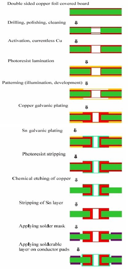
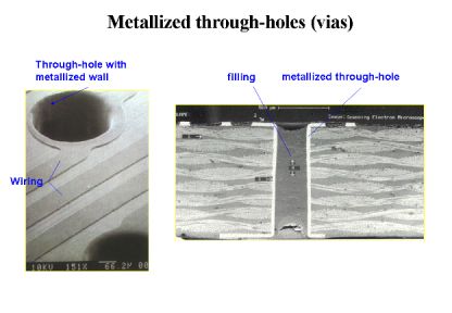
Technology of double-sided PWBs The basic process for producing a double-sided through-hole connected PWB is called pattern plating. This sequence includes main groups of processing steps as follows: - Starting with a double-sided copper clad laminate, at first, holes are fabricated by drilling, and then they are deburred and cleaned. - The panels are sensitized and an electroless copper flash is given to make the holes conductive for electroplating. A plating-resistant negative mask is produced by lamination and transferring the image, and a pattern of copper layer is electroplated to the uncovered areas. The minimum thickness of the copper layer required in the holes is usually 20 m. At this point it should be mentioned, that a modern electrochemical process called direct plating, that combines electroless plating and electroplating to be carried out in the same bath, and thus simplifies the processing sequence, is also in use. - A second metal, a tin-lead solder is electroplated over the copper to act as an etch-resistant mask, to improve solderability and to provide protection against the corrosion of the copper layer. - The photoprinted mask is stripped, and the copper layer is etched to get the required pattern. - Finally the tin-lead coating is reflowed to cover and protect the edges of the copper layer, and to improve the overall appearance of the board. This solder reflow is usually carried out by blowing hot air to the surface, and the process is called hot air leveling. Manufacturing sequences of double-sided PWBs
The second manufacturing route used for double-sided printed wiring boards is known as panel plating. The main steps are as follows: drilling of holes and cleaning; activation and deposition of electroless copper; electroplating copper across the whole panel; laminating with photoresist; image transfer by exposure and developing; electroplating of tin-lead solder; removal of photoresist; etching of unprotected copper; and reflow of the solder coating.
|
 PWB Types and Materials